

Radiating packaging structure of semiconductor chip
A semiconductor and chip technology, applied in the direction of semiconductor devices, semiconductor/solid-state device parts, electric solid-state devices, etc., can solve problems such as limiting the application range of heat dissipation design
- Summary
- Abstract
- Description
- Claims
- Application Information
AI Technical Summary
Problems solved by technology
Method used
Image

Examples
Embodiment Construction
[0027] In order to make the above-mentioned purposes, features and advantages of the present invention more obvious and understandable, the preferred embodiments of the present invention will be specifically cited below, together with the accompanying drawings, for a detailed description as follows:
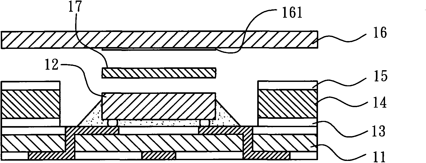
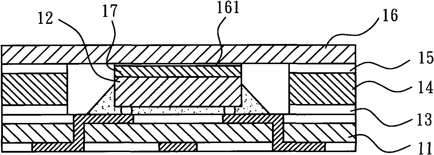
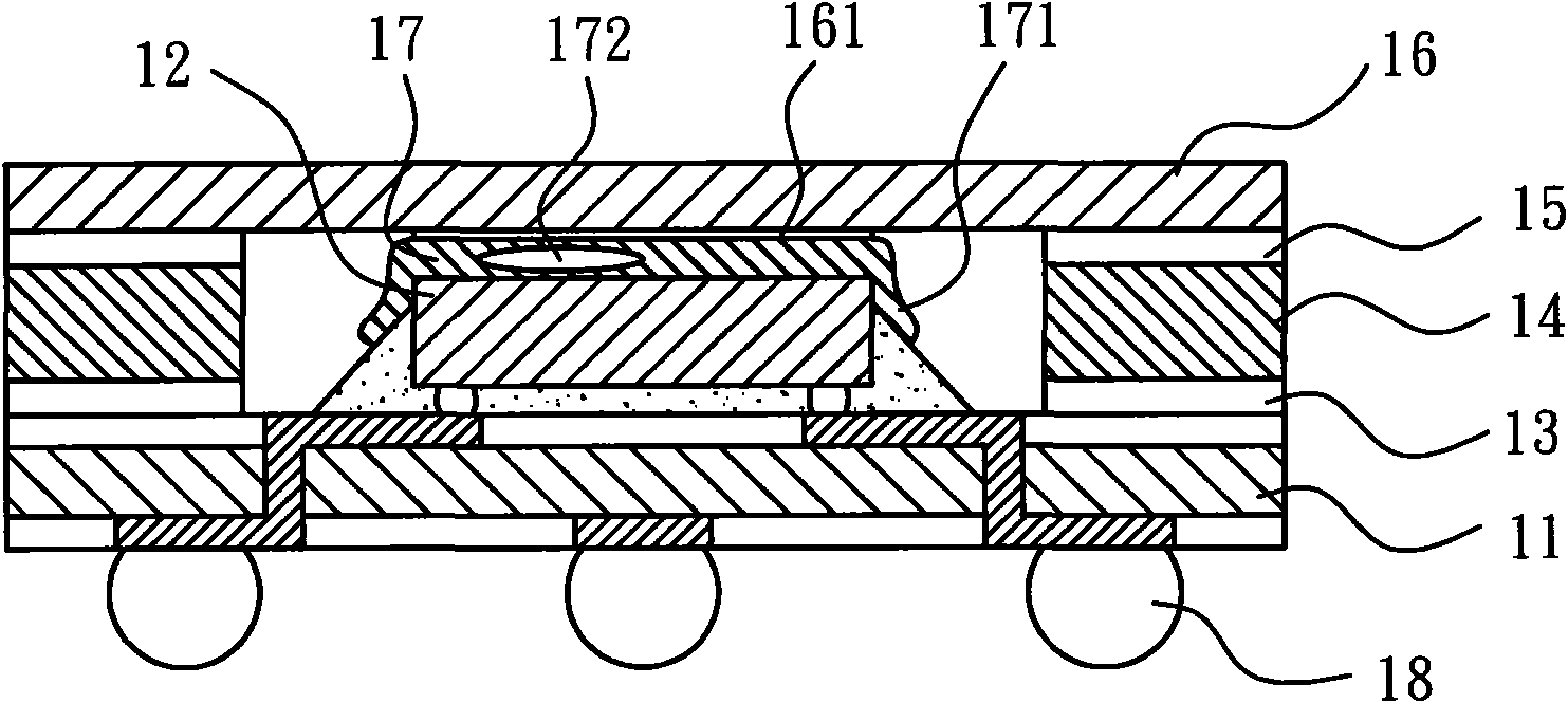
[0028] Please refer to Figure 2A , 2B and 2C, which disclose an assembly schematic diagram of a heat dissipation package structure for a semiconductor chip according to the first embodiment of the present invention, wherein the heat dissipation package structure includes a substrate 21, at least one chip 22, a first adhesive layer 23, a frame 24, A second adhesive layer 25 , a heat sink 26 , a thermal interface material layer 27 and several output terminals 28 . The present invention is applicable to common package structures with substrates, such as ball grid array package structure (BGA), pin grid array package structure (PGA), land grid array package structure (LGA) or chip-...
PUM
 Abstract
Description
Claims
Application Information