Organic light-emitting diode (OLED) display screen

A technology of light-emitting diodes and organic light-emitting layers, which can be used in static indicators, identification devices, semiconductor/solid-state device components, etc., and can solve the problems of increasing production costs and manufacturing process difficulties, limiting the scope of application, increasing the number of layers of organic light-emitting diodes, etc. problem, achieve the effect of reducing production cost and manufacturing difficulty, clear image display, and precise touch operation

Active Publication Date: 2010-11-24
SHANGHAI TIANMA MICRO ELECTRONICS CO LTD
View PDF1 Cites 74 Cited by
  • Summary
  • Abstract
  • Description
  • Claims
  • Application Information

AI Technical Summary

Problems solved by technology

[0015] The present invention aims to solve the technical problems of the corresponding increase in production cost and manufacturing process difficulty due to the large increase in the number of organic light-emitting diode (OLED) layers caused by the integration of capacitive touch screens in the prior art, and only the prior art Only when the capacitive touch screen is integrated into the top-emitting OLED display, technical problems such as limiting the scope of application

Method used


Image

  • Organic light-emitting diode (OLED) display screen
  • Organic light-emitting diode (OLED) display screen
  • Organic light-emitting diode (OLED) display screen

Examples


Embodiment 1

[0065] This embodiment provides a bottom-emitting OLED display integrated with a capacitive touch screen.

[0066] See Figure 4A , which is a schematic diagram of the layer structure of the bottom emission OLED display integrated with the capacitive touch screen provided by Embodiment 1 of the present invention.

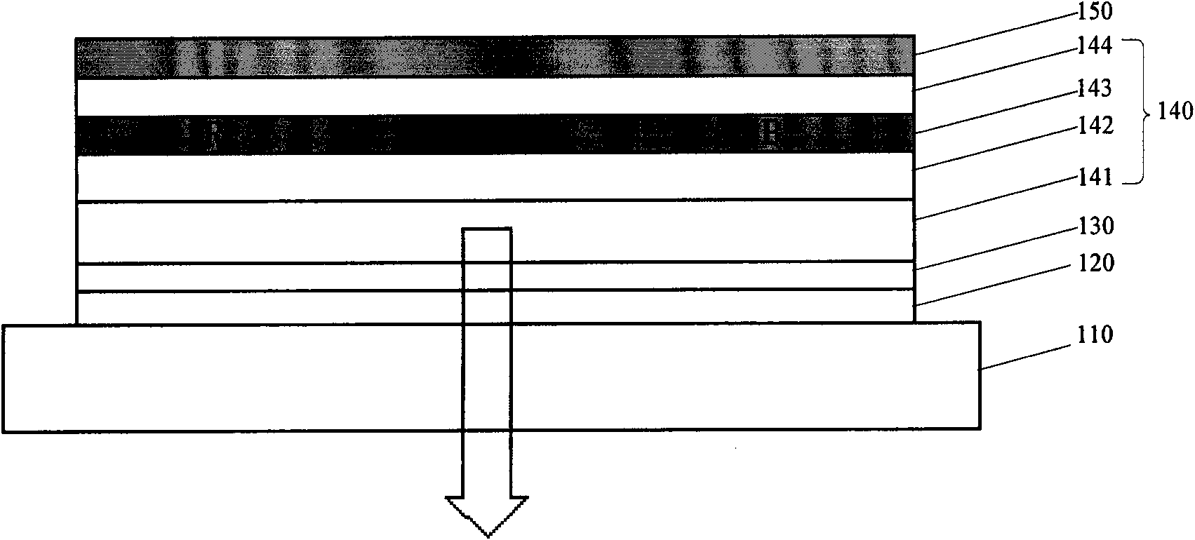
[0067] The bottom-emission OLED display includes a glass substrate 410 , a circuit layer 420 , an anode layer 430 , an organic light-emitting layer 440 , and a cathode layer 450 stacked on one side of the glass substrate 410 from bottom to top. The organic light emitting layer 440 is composed of a hole injection layer 441 , a hole transfer layer 442 , an organic layer 443 , and an electron transfer layer 444 .

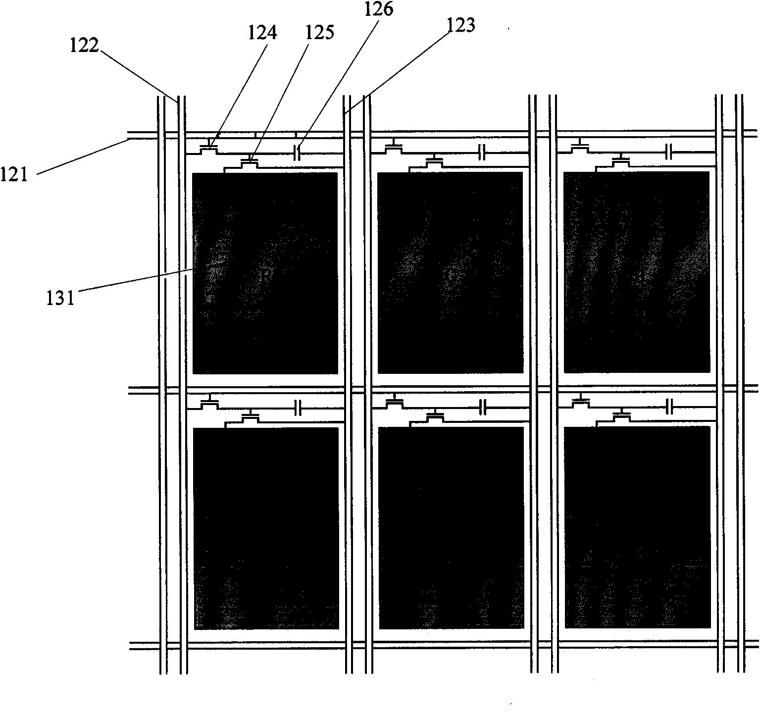
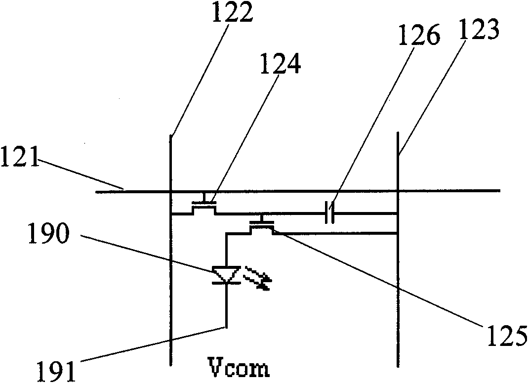
[0068] The bottom-emission OLED display further includes a touch sensing layer 400, which is disposed on the other side of the glass substrate 410, and uses an anode layer 430 as a driving layer for touch sensing, wherein the anode layer 430 is coupled to t...

Embodiment 2

[0082] This embodiment provides a capacitive touch screen integrated in a top-emitting OLED display.

[0083] See Figure 5A , which is a schematic diagram of the layer structure of the capacitive touch screen integrated in the top-emitting OLED display provided by the second embodiment of the present invention.

[0084] The capacitive touch screen is sequentially stacked with a substrate 510, a circuit layer 520, a cathode layer 530, an anode layer 550, a glass substrate 560, and a touch sensing layer 500 from bottom to top, wherein the touch sensing layer 500 uses the anode layer 550 as the driver layer. In the present invention, the touch sensing layer 500 is preferably formed of indium tin oxide (ITO).

[0085] In this embodiment, the organic light-emitting layer 540 includes an electron transfer layer 541, an organic layer 542, a hole transfer layer 543, and a hole injection layer 544,

[0086] In this embodiment, the protection layer 570 is disposed on the side of the...

Embodiment 3

[0098] This embodiment provides another capacitive touch screen integrated in a top-emitting OLED display,

[0099] See Figure 6 , which is a schematic diagram of the layer structure of the capacitive touch screen integrated in the top-emitting OLED display provided by the third embodiment of the present invention.

[0100] The capacitive touch screen is sequentially stacked with a substrate 610, a circuit layer 620, a cathode layer 630, an organic light-emitting layer 640, an electron transfer layer 641, an organic layer 642, a hole transfer layer 643, a hole injection layer 644, and an anode layer. The layer 650, the glass substrate 660, and the touch sensing layer 600 are disposed between the glass substrate 660 and the anode layer 650, and the anode layer 650 is used as a driving layer.

[0101] Its working principle is the same as that of the second embodiment above, and will not be repeated here.

[0102] The top-emitting OLED display integrated with a capacitive touc...


PUM


Abstract

The invention provides an organic light-emitting diode (OLED) display screen. The display screen comprises a glass substrate, a circuit layer, an anode layer, an organic luminescent layer, a cathode layer, a touch control inductive layer and a touch control detection unit, wherein the circuit layer, the anode layer, the organic luminescent layer and the cathode layer are arranged on one side of the glass substrate. The OLED display screen integrated with a capacitive touch screen provided by the invention can perform accurate touch control operation and clear image display at the same time. Compared with the prior art, the display screen has the advantages of reducing a plurality of structural layers and effectively lowering production cost and manufacturing difficulty. Moreover, the capacitive touch screen can be integrated in a bottom luminous OLED display screen structure so that the application range of technology can be expanded greatly.

Description

technical field [0001] The invention relates to the field of display and touch technology, in particular to an organic light emitting diode display integrated with a capacitive touch screen. Background technique [0002] OLED stands for Organic Light-Emitting Diode (Organic Light-Emitting Diode), also known as Organic Electroluminesence Display (OLED). Since 2003, this kind of display device has been widely used in MP3 players because of its features such as thinness and power saving. OLED display has many incomparable advantages of LCD, so it has been favored by industry insiders. . [0003] The basic structure of an OLED display is a thin, transparent Indium Tin Oxide (ITO) with semiconducting properties, connected to the positive electrode of electricity, plus another metal cathode, wrapped into a sandwich structure. The whole structural layer includes: hole transport layer (HTL), light emitting layer (EL) and electron transport layer (ETL). When the power is supplied ...

Claims


Application Information

Patent Timeline
Patent Type & Authority Applications(China)
IPC IPC(8): H01L27/32H01L23/52G09F9/33G09G3/32G06F3/033G06F3/0354G09G3/3225
CPCH01L27/323H10K59/40H10K59/12H10K59/805
Inventor 陈悦邱承彬吴显浩王丽花于祥国
Owner SHANGHAI TIANMA MICRO ELECTRONICS CO LTD
Why Eureka
Try Eureka