
Clock pulse signal generation method

A clock pulse and signal generation technology, applied in the field of clock pulse signal generation, can solve problems such as insufficient pixel charging rate, waveform distortion, pixel P loss of brightness, etc., and achieve the effect of improving display quality

Inactive Publication Date: 2012-08-29
AU OPTRONICS CORP
View PDF0 Cites 0 Cited by
  • Summary
  • Abstract
  • Description
  • Claims
  • Application Information

AI Technical Summary

Problems solved by technology

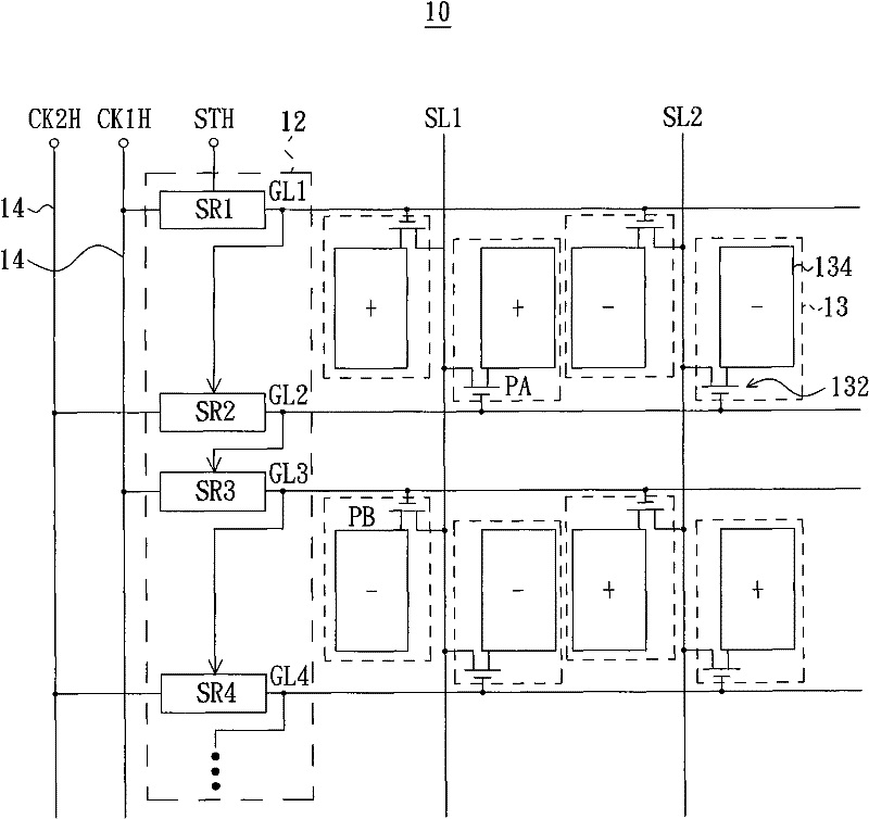
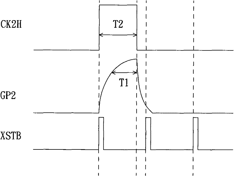
exist figure 2 Among them, GP2 is the gate drive signal provided to the gate line GL2, and XSTB is the polarity inversion enabling signal of the display data on the data lines SL1 and SL2; It is coupled to the bus 14 to receive the two-phase clock pulse signals CK1H, CK2H. Therefore, when any clock pulse signal such as CK2H is transmitted on the bus, there will be a rising edge (Rising edge) distortion due to the effect of parasitic capacitance, so that the gate The waveform of the driving signal GP2 will generate corresponding distortion, which will cause the pixel P electrically connected to the gate line GL2 A The effective charging time T1 of the pixel will be less than the ideal charging time T2, that is, the pixel charging rate (chargingratio) is less than expected, and the pixel P A will lose the brightness it should have; here, every rising edge of the polarity inversion enabling signal XSTB will trigger a polarity inversion of the display data on the data lines SL1 and SL2
Additionally, from figure 2 It can also be found that, due to the falling edge of the gate drive signal GP2, there may be a dragging phenomenon, so that the pixel P A The pixel P A will be written to the pixel P that should be written B display data, thus affecting the pixel P A The brightness and / or color of the
[0006] Therefore, how to avoid insufficient charging rate of pixels and / or drag phenomenon on the falling edge of the gate drive signal caused by waveform distortion caused by the effect of parasitic capacitance on the clock pulse signal is one of the important problems to be solved urgently. display quality

Method used


Image

  • Clock pulse signal generation method
  • Clock pulse signal generation method
  • Clock pulse signal generation method

Examples


Embodiment Construction

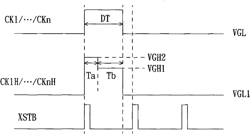
[0053] see image 3 , which shows a timing diagram of multiple signals related to a method for generating a clock pulse signal according to an embodiment of the present invention. The method for generating the clock pulse signal in this embodiment is suitable to be implemented in a display, such as an active matrix display using an on-array gate driving circuit and / or a half-source driving structure, but the present invention is not limited thereto. The following will combine image 3 Each step of the method for generating a clock pulse signal in this embodiment will be described in detail.

[0054] First, at least one initial clock pulse signal CK1˜CKn is provided, where n is a positive integer. image 3 The waveform of any one of the initial clock pulse signals CK1~CKn is shown in , the duty period DT of the initial clock pulse signals CK1~CKn in each frequency period (not marked) has an initial high potential VGH, and in this frequency period The non-responsible period (...


PUM


Abstract

The invention relates to a clock pulse signal generation method, which is performed on a display. Specifically, the clock pulse signal generation method comprises the steps of: providing at least one initial clock pulse signal, which includes an initial high potential in a duty cycle within a frequency cycle; and performing potential shifting operation on the initial clock pulse signal so that the initial high potential of the initial clock pulse signal is respectively shifted to a first high potential and a second high potential in a first time period and a second time period within the dutycycle, thereby resulting in at least one new clock pulse signal which is used by a grid drive circuit of the display to generate a grid drive signal, wherein the first time period is earlier than thesecond time period, and the first high potential is larger than the second high potential.

Description

technical field [0001] The present invention relates to the field of display technology, and in particular relates to a method for generating a clock pulse signal to provide a satisfactory clock pulse signal for a gate drive circuit in a display to generate a gate drive signal. Background technique [0002] Active-matrix flat-panel displays such as active-matrix liquid crystal displays are widely used in consumer electronics such as mobile phones, notebook computers, desktop monitors, and televisions due to their advantages of high image quality, small size, light weight, and wide application range. , and has gradually replaced the traditional cathode ray tube (CRT) display and has become the mainstream of the display. [0003] In order to make the display product thinner and its cost more competitive, it is proposed in the prior art to use a gate-on-array (Gate-On-Array, GOA) drive circuit directly formed on the display array substrate to generate gate drive signal and / or ...

Claims


Application Information

Patent Timeline
Patent Type & Authority Patents(China)
IPC IPC(8): G09G3/20
CPCG09G5/18G09G3/3648G09G3/3677G09G2310/067G09G2310/08
Inventor 郑晓锺萧开元
Owner AU OPTRONICS CORP
Learn More