Memory interface method based on CLB (Central Logic Bus) bus

A memory interface and memory technology, applied in instruments, electrical digital data processing, etc., can solve problems such as occupation, not improving work efficiency, etc., and achieve the effect of prolonging the latching time, improving the clock utilization rate, and reducing the number of waiting cycles.

Active Publication Date: 2010-12-22
苏州国芯科技股份有限公司
View PDF4 Cites 6 Cited by
  • Summary
  • Abstract
  • Description
  • Claims
  • Application Information

AI Technical Summary

Problems solved by technology

image 3 Although the high-speed memory interface mode triggered by the falling edge shown in the figure achieves high-speed reading and writing, which meets the high-frequency requirements, it takes two clock cycles for each read (write) operation of the memory, which is practical. Didn't improve work efficiency much

Method used


Image

  • Memory interface method based on CLB (Central Logic Bus) bus
  • Memory interface method based on CLB (Central Logic Bus) bus
  • Memory interface method based on CLB (Central Logic Bus) bus

Examples


Embodiment

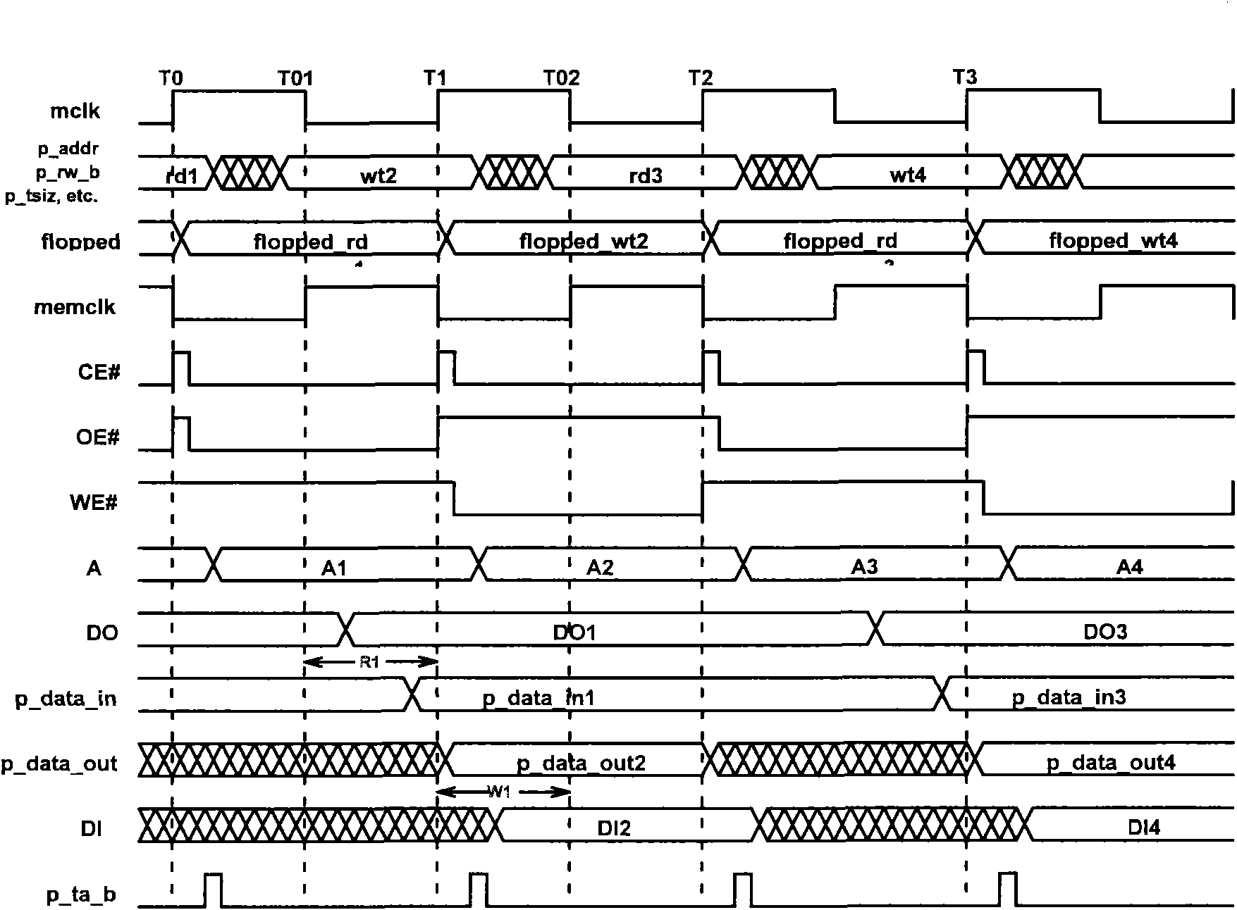
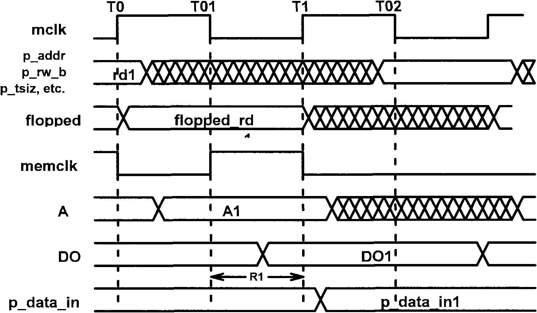
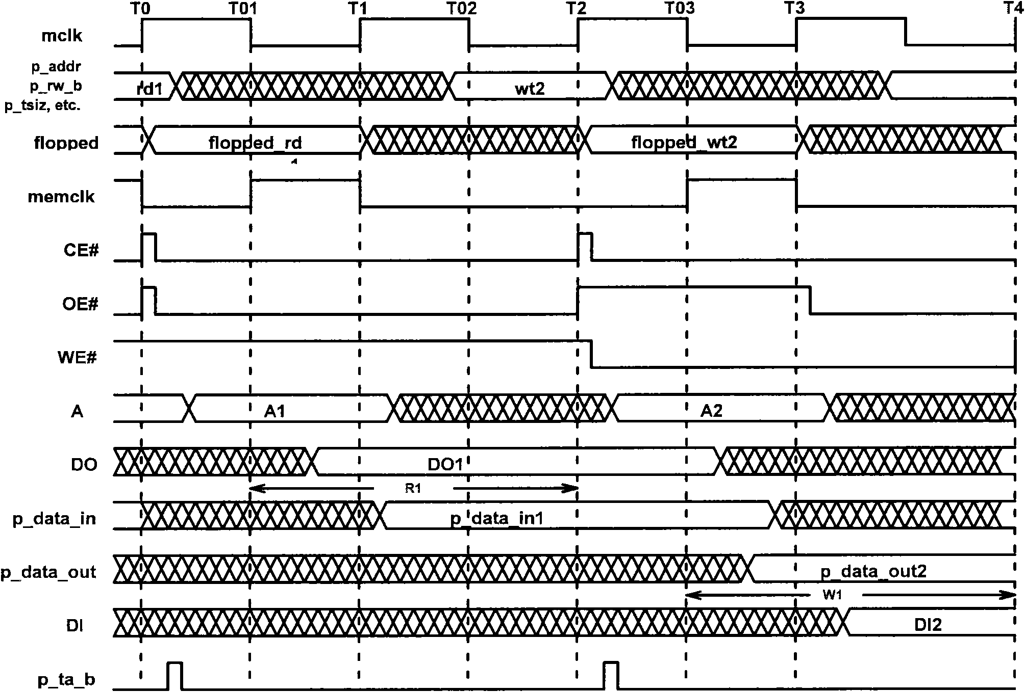
[0027] Embodiment: a kind of memory interface method based on CLB bus,

[0028] Including: on the rising edge of the bus clock m_clk, the processor sends a read or write operation request, and the bus latches the address signal and control signal from the processor to obtain the first latch signal, and generates a memory enable signal; at the same time, the address Inputs for transmission of signals and control signals to the memory;

[0029] After the rising edge of the bus clock, the adjacent falling edge latches the address and control signal again to obtain the second latch signal. At this time, the memory generates the memory clock mem_clk according to the memory enable signal, and the falling edge of the memory clock mem_clk Synchronized with the falling edge of the bus clock m_clk; at the same time, the memory receives the first latch signal or the second latch signal from the bus;

[0030] After the falling edge of the memory clock mem_clk, when a read operation is pe...


PUM


Abstract

The invention discloses a memory interface method based on a CLB (Central Logic Bus) bus, comprising the following steps of, at a rising edge of a bus clock, sending a reading or writing operation request by a processor, latching address signals and control signals from the processor by the bus to obtain first latching signals, and generating enabling signals of a memory; at a falling edge arranged behind and adjacent to the rising edge of the bus clock, generating a memory clock according to the enabling signals of the memory by the memory, wherein a falling edge of the memory clock is synchronous with the falling edge of the bus clock; behind the falling edge of the memory clock, in the reading operation, outputting data to achieve the data output end of the memory, delaying by a line, and achieving the data input end of the processor in the front of an adjacent rising edge behind the rising edge of the bus clock; in the writing operation, writing data to achieve the data output end of the processor, delaying by the line, and achieving the data input end of the memory in the front of the adjacent rising edge behind the rising edge of the bus clock. When realizing high-speed reading or writing operation of the memory, the invention efficiently reduces the amount of waiting period and enhances the clock utilization.

Description

technical field [0001] The invention relates to a memory interface method based on a CLB bus. Background technique [0002] In embedded chip design, memory is usually attached to the system bus as a storage space for data or variables. In terms of application form, the main device, bus, memory interface and memory can be on the same chip at the same time, or one or several devices can be on the same chip and the other one or several devices can be on the FPGA. There are differences, which cause the memory to have a more flexible interface connected to the system bus. With the continuous development of technology, the requirements for reading and writing of memory are getting higher and higher, so the requirements for reading and writing of high-speed memory are more stringent. [0003] For the C*CORE series 32-bit microprocessor bus (CLB bus) of Suzhou Guoxin Technology Co., Ltd., its interface technology to the memory adopts the falling edge mode. Its operation sequence ...

Claims


Application Information

Patent Timeline
Patent Type & Authority Applications(China)
IPC IPC(8): G06F13/16
Inventor 郑茳肖佐楠竺际隆陈霞林峰
Owner 苏州国芯科技股份有限公司
Why Eureka
Try Eureka