Semiconductor package with electromagnetic interference protection cover

An electromagnetic interference, semiconductor technology, applied in the direction of semiconductor devices, semiconductor/solid-state device manufacturing, semiconductor/solid-state device components, etc., can solve the problems of increasing manufacturing costs and manufacturing time, time-consuming, and expensive manufacturing processes.

Active Publication Date: 2010-12-29
ADVANCED SEMICON ENG INC
View PDF0 Cites 20 Cited by
  • Summary
  • Abstract
  • Description
  • Claims
  • Application Information

AI Technical Summary

Problems solved by technology

Positioning the case and encapsulant to match the size and shape of the case and encapsulant can make the manufacturing process more expensive and time consuming
In addition, semiconduct...

Method used

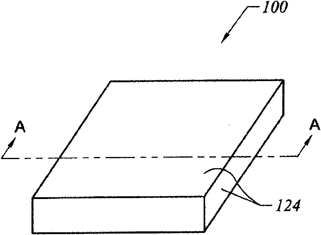
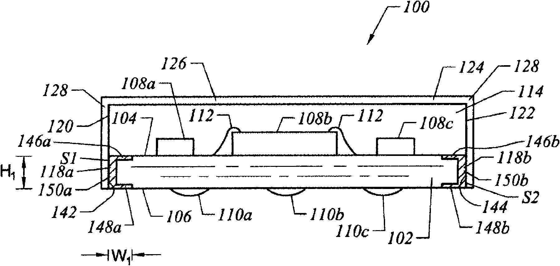
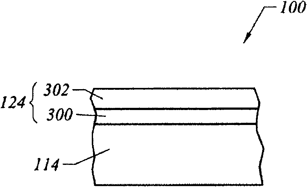

Image

  • Semiconductor package with electromagnetic interference protection cover
  • Semiconductor package with electromagnetic interference protection cover
  • Semiconductor package with electromagnetic interference protection cover

Examples


Embodiment Construction

[0059] The following definitions apply in relation to several embodiments of the present invention. Such definitions may likewise be extended here.

[0060] As used herein, statements in the singular form of "a" and "the" include the plural unless the context clearly dictates otherwise. Therefore, for example, unless the context clearly states otherwise, a ground component may include several ground components.

[0061] As used herein, a "set" means a collection of one or more components. For example, a set of layer structures may comprise a single layer structure or a multilayer structure. A component in a group may refer to a member of the group. Components in a set can be the same or different. In some examples, components in a group may share one or more common characteristics.

[0062] As used herein, the term "adjacent" means near or adjacent. Adjacent components may be separated from each other or may be in actual or direct contact with each other. In some exampl...


PUM

PropertyMeasurementUnit
Heightaaaaaaaaaa
Widthaaaaaaaaaa
Thicknessaaaaaaaaaa

Abstract

The invention provides a semiconductor package with an electromagnetic interference protection cover and a related method. In one embodiment, the semiconductor package comprises: (1) a substrate unit comprising a grounding component; (2) a semiconductor component configured nearby the upper surface of the substrate unit; (3) sealing colloid configured nearby the upper surface of the substrate unit and covered on the semiconductor component; and (4) the electromagnetic interference protection cover configured nearby the outside surface of the sealing colloid and electrically connected with the connection surface of the grounding component. The side surface of the sealing colloid is essentially aligned with the side surface of the substrate unit, and the connection surface of the grounding component is adjacent to the side surface of the substrate unit and is electrically exposed. The grounding component is provided with an electric channel, so that electromagnetic radiation on the electromagnetic interference protection cover is discharged to a grounding end.

Description

technical field [0001] The present invention relates to a semiconductor package, and more particularly to a semiconductor package with an electromagnetic interference shield. Background technique [0002] Semiconductor devices have gradually become more complex, partly because the demand for semiconductor devices has gradually trended toward smaller size and higher processing speed. Although semiconductor devices with small size and high processing speed characteristics have many advantages, these characteristics also cause many problems. Specifically, when the clock speed increases, the transition between signal levels may increase, resulting in an increased level of electromagnetic radiation, and making the electromagnetic radiation higher in frequency or shorter in wavelength. Electromagnetic emissions can be emitted by a source semiconductor device and can affect adjacent semiconductor devices. When the electromagnetic radiation located adjacent to the semiconductor de...

Claims


Application Information

Patent Timeline
IPC IPC(8): H01L23/552H01L23/58H01L21/50H01L21/56H01L21/60H05K9/00
CPCH01L24/97H01L2924/15311H01L2924/19105H01L2924/01029H01L2924/01047H01L2924/01079H01L2224/16225H01L2224/97H01L2924/01013H01L2924/3025H01L2924/01024H01L2224/48227H01L21/568
Inventor 廖国宪邱基综洪志斌
Owner ADVANCED SEMICON ENG INC
Why Eureka
Try Eureka