High-bandwidth high-isolation low on-resistance CMOS analog switch circuit and realizing mode thereof

A low on-resistance, high-isolation technology, applied in electronic switches, electrical components, pulse technology, etc., to achieve the effect of improving transmission bandwidth, wide bandwidth, and low on-resistance

Inactive Publication Date: 2010-12-29
上海英联电子科技有限公司
View PDF0 Cites 16 Cited by
  • Summary
  • Abstract
  • Description
  • Claims
  • Application Information

AI Technical Summary

Problems solved by technology

[0003] The invention solves the problem of the mutual restriction of the on-resistance and the transmission bandwidth of the traditional CMOS analog switch circuit, greatly improves the transmission bandwidth of the CMOS analog switch under the same on-resistance without affecting the isolation

Method used


Image

  • High-bandwidth high-isolation low on-resistance CMOS analog switch circuit and realizing mode thereof
  • High-bandwidth high-isolation low on-resistance CMOS analog switch circuit and realizing mode thereof
  • High-bandwidth high-isolation low on-resistance CMOS analog switch circuit and realizing mode thereof

Examples


Embodiment Construction

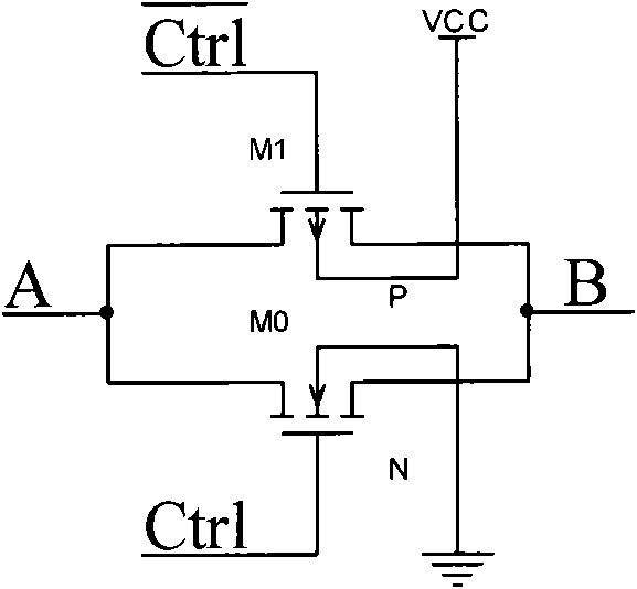
[0011] As shown in Figure 1, the traditional CMOS analog switch circuit is composed of paired NMOS and PMOS in parallel. Its gate is connected to control signal, and its substrate is grounded and power supply respectively.

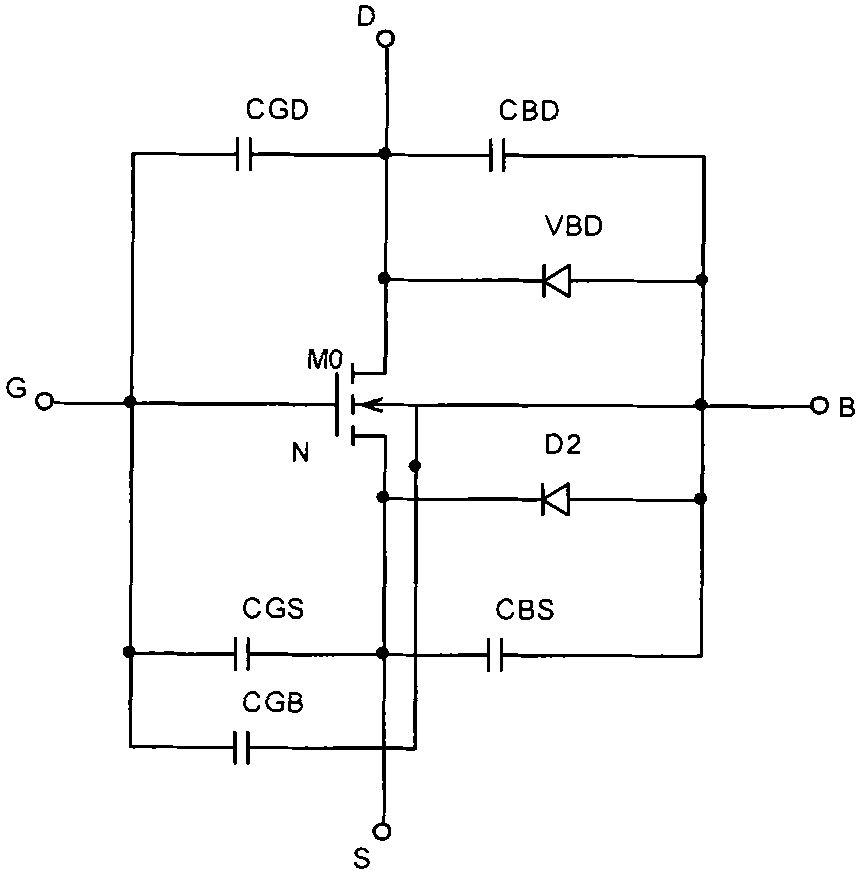
[0012] As shown in Figure 2, the traditional CMOS analog switch transmits signals through C GD 、C GS 、C GB 、C BD 、C BS Receive the AC signal ground respectively. As the size of the CMOS analog switch increases, the on-resistance decreases, and the C GD 、C GS 、C GB 、C BD 、C BS It is increasing, which affects the transmission of high-frequency signals.

[0013] Due to the separation of B and S in the traditional CMOS analog switch, there is a lining offset effect, which affects V T

[0014] V T = V T 0 + γ ( 2 | φ F | ...


PUM


Abstract

The invention provides a CMOS switch circuit with wider bandwidth, high isolation and low on-resistance, which is used for multi-path high-frequency analog signal switching. By adopting the technology of floating trap and grid impedance control, the problem that the on-resistance and the transmission bandwidth of the traditional CMOS analog switch circuit are restricted with each other can be solved, so that the signal transmission bandwidth of the CMOS switch under the same on-resistance and isolation can be greatly improved.

Description

technical field [0001] . The present invention is a CMOS analog switch circuit for switching multiple analog signals, which has the technical characteristics of wide bandwidth, high isolation and low conduction resistance. Background technique [0002] Currently, many devices need to switch multiple signals. Such as the switching of multiple SIM cards in mobile phones, the switching of different audio signals; the switching of sampling signals in measuring equipment. The frequency of the switched signal is very wide, ranging from several kilohertz to several megahertz, or even tens or hundreds of megahertz. Traditional CMOS analog switches have either low on-resistance and low bandwidth, or high on-resistance and high bandwidth. Current high-speed analog signal switching requires analog switches with low on-resistance and low parasitic capacitance at the same time. Contents of the invention [0003] The invention solves the problem of mutual restriction between the on-r...

Claims


Application Information

Patent Timeline
Patent Type & Authority Applications(China)
IPC IPC(8): H03K17/687
Inventor 杨永华陈碧葛利明吴蕾
Owner 上海英联电子科技有限公司
Why Eureka
Try Eureka