Combined environment test method for integrated circuit

A technology of integrated circuits and test methods, which is applied in the field of integrated circuits, can solve problems such as the inability to truly simulate the use environment of integrated circuits, and achieve the effect of accurate evaluation

Inactive Publication Date: 2011-01-26
BEIJING SHENGTAOPING TEST ENG TECH RES INST
View PDF0 Cites 22 Cited by
  • Summary
  • Abstract
  • Description
  • Claims
  • Application Information

AI Technical Summary

Problems solved by technology

[0003] The purpose of the present invention is to provide a method for comprehensive environmental testing of integrated ci

Method used


Image

  • Combined environment test method for integrated circuit
  • Combined environment test method for integrated circuit
  • Combined environment test method for integrated circuit

Examples


Embodiment Construction

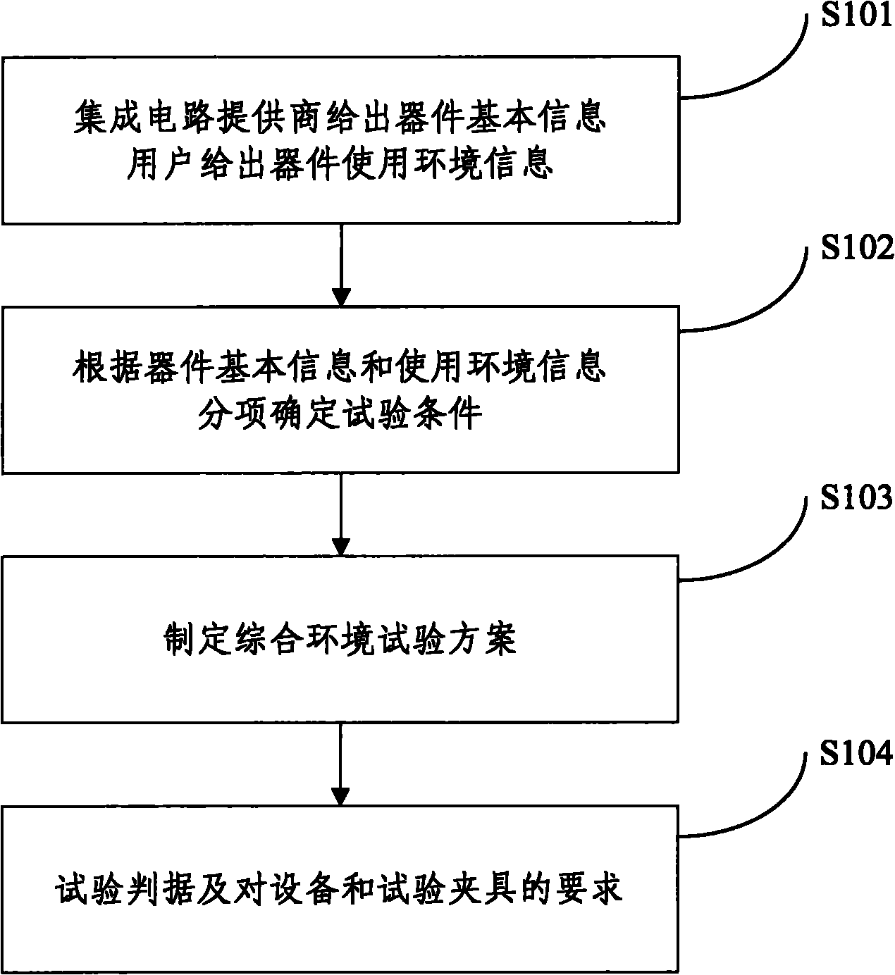
[0025] The following examples are used to illustrate the present invention, but are not intended to limit the scope of the present invention.

[0026] figure 1 It is a flow chart of an embodiment of the integrated circuit comprehensive environmental test method of the present invention, and the test method of the present embodiment includes the following steps:

[0027] S101. The integrated circuit provider provides basic information of the product, and the user provides information on the environment in which the device (integrated circuit) is used as an input for formulating comprehensive test conditions.

[0028] The basic product information that the integrated circuit supplier should provide includes: the maximum operating temperature of the device, the minimum operating temperature of the device, the rated operating voltage of the device, the maximum operating voltage of the device, and the minimum operating voltage of the device, etc.

[0029] The user provides the env...


PUM


Abstract

The invention discloses a combined environment test method for an integrated circuit, which comprises the following steps of: S1) acquiring the highest test temperature, the lowest test temperature, the highest test temperature change rate delta TE, a test power density spectrum, a test humidity and a test electric stress according to the basic product information of the integrated circuit and the used environment information, S2) according to the test data, performing a temperature cycling test, a random vibration test and a humid test while respectively exerting a rated operational voltage, the maximum operating voltage and the minimum operating voltage on the integrated circuit, and S3) after finishing the tests, performing a functional test on the integrated circuit, confirming the integrated circuit invalid if the integrated circuit loses the function or any property parameter value exceeds a designed scope, otherwise, confirming the integrated circuit being in good condition. The invention can really simulate the actual using environment of the integrated circuit, quickly and completely arouse the faults of the products and provide a reference to improve the design and the manufacturing shortcomings of the integrated circuit.

Description

technical field [0001] The invention relates to the technical field of integrated circuits, in particular to a comprehensive environmental test method for integrated circuits. Background technique [0002] Integrated circuits will be subjected to various environmental stresses in actual use, and the weak links of products are easily exposed under the action of such comprehensive environmental stresses. In recent years, large-scale integrated circuit development units and users have proposed on different occasions that there is an urgent need for test methods that can quickly and effectively evaluate the quality and reliability of large-scale integrated circuits. The data show that among the many environmental factors that have the greatest impact on product quality and reliability are temperature (40%), vibration (28%) and humidity (18%), humidity refers to relative humidity, that is, the actual water vapor density in the air and the percentage value of saturated water vapo...

Claims


Application Information

Patent Timeline
IPC IPC(8): G01R31/28
Inventor 王群勇阳辉吴文章白桦陈冬梅陈晓陈宇刘燕芳
Owner BEIJING SHENGTAOPING TEST ENG TECH RES INST
Why Eureka
Try Eureka