Active matrix substrate, display device, method for inspecting active matrix substrate and method for inspecting display device
一种有源矩阵、显示装置的技术,应用在测量装置、辨认装置、光学等方向,能够解决液晶面板100b显示品质下降等问题,达到提高显示品质的效果
- Summary
- Abstract
- Description
- Claims
- Application Information
AI Technical Summary
Problems solved by technology
Method used
Image

Examples
Embodiment Construction
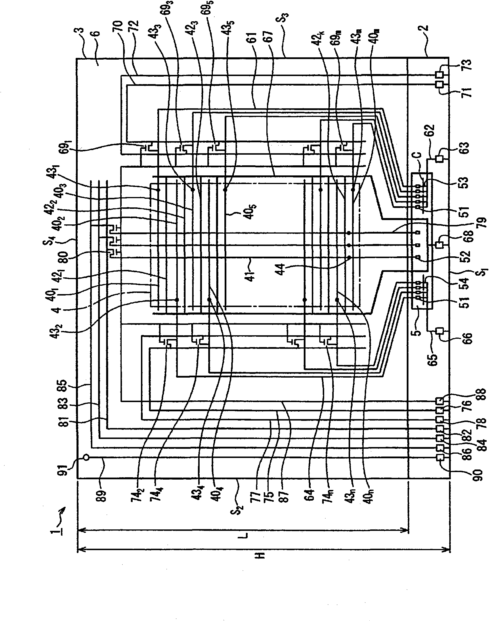
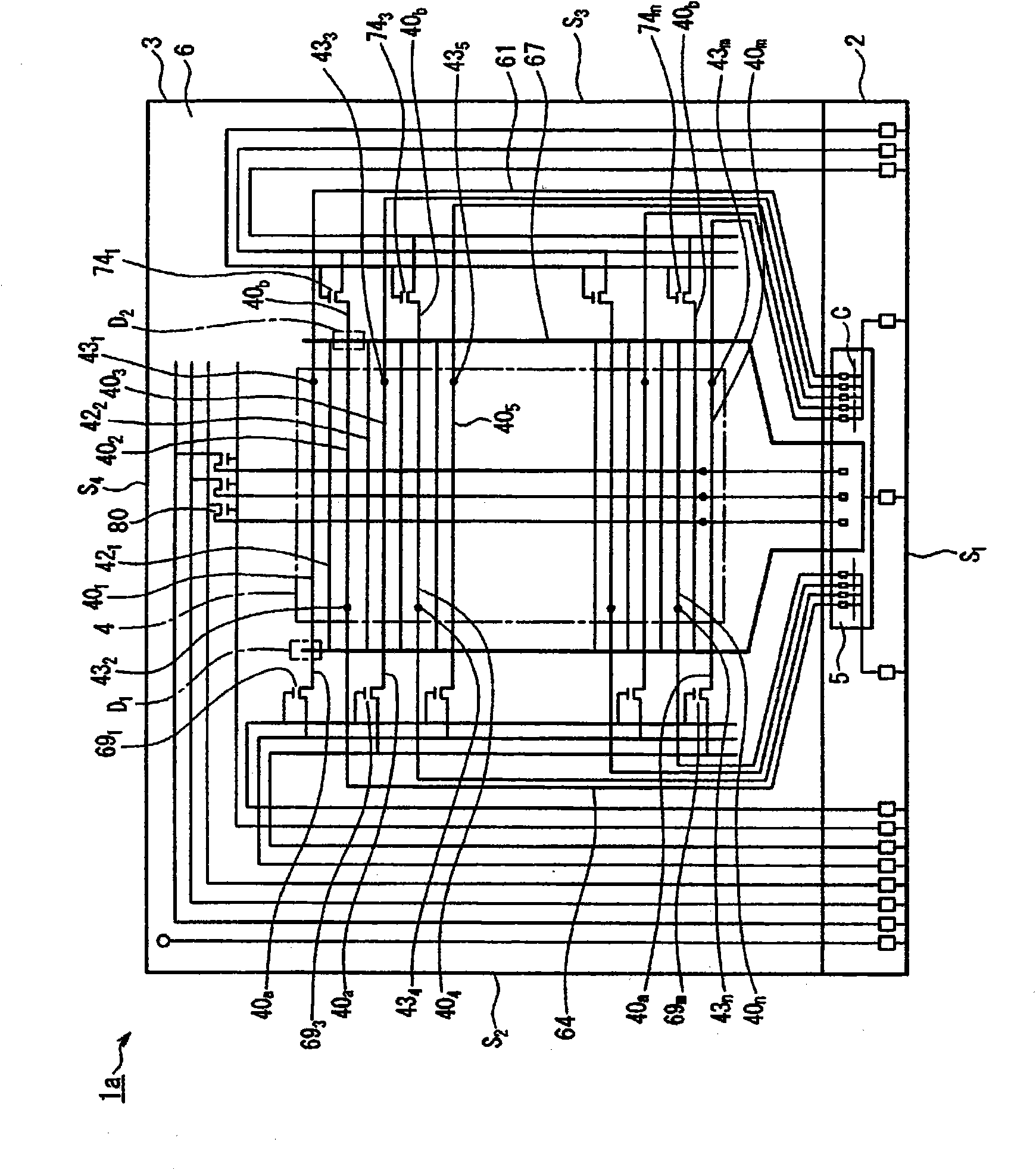
[0049] An active matrix substrate according to an embodiment of the present invention includes: a plurality of scanning wirings formed in parallel with each other in a display area; and a plurality of scanning wirings formed in parallel with each other in the display area. Data wiring; and multiple scan terminals and multiple data terminals arranged in the terminal configuration area. The plurality of scanning wirings described above includes: a plurality of first scanning wirings having an input terminal of a scanning signal on one end side; and a plurality of second scanning wirings having an input terminal of a scanning signal on the other end side. In the display area, the first scan wiring and the second scan wiring are alternately formed each. The active matrix substrate includes: a plurality of first connection wirings connecting the scanning signal input ends of the first scanning wiring and the scanning terminal; and connecting the scanning signal input ends of the sec...
PUM
 Abstract
Description
Claims
Application Information
 - Generate Ideas
- Intellectual Property
- Life Sciences
- Materials
- Tech Scout
- Unparalleled Data Quality
- Higher Quality Content
- 60% Fewer Hallucinations
Browse by: Latest US Patents, China's latest patents, Technical Efficacy Thesaurus, Application Domain, Technology Topic, Popular Technical Reports.
© 2025 PatSnap. All rights reserved.Legal|Privacy policy|Modern Slavery Act Transparency Statement|Sitemap|About US| Contact US: help@patsnap.com