Light emitting diode (LED) and encapsulating method thereof

A packaging method and a technology of external sealing glue, which is applied in the direction of electrical components, electric solid devices, circuits, etc., can solve problems such as uneven light, uneven light output from LEDs, and uneven amount of glue on the top of the LED chip, and achieve uniform light output. Effect

Active Publication Date: 2011-02-16
LEDMAN OPTOELECTRONICS
View PDF4 Cites 10 Cited by
  • Summary
  • Abstract
  • Description
  • Claims
  • Application Information

AI Technical Summary

Problems solved by technology

[0004] However, the thickness of the above-mentioned outer sealant (not shown) applied on the surface of the LED chip is inconsistent, that is, the space above the height of the fixed LED chip in the metal cup is different from the space above the height of the unfixed LED chip, so the outer sealant is applied. The thickness of the sealing glue is also inconsistent, and the viscosity of the outer sealing glue and the amount of glue above the LED chip are not uniform, so that the surface of the entire packaging glue is not on a horizontal plane, which is easy to cause uneven light emitted by the LED, which also leads to the overall LED light is not uniform

Method used


Image

  • Light emitting diode (LED) and encapsulating method thereof
  • Light emitting diode (LED) and encapsulating method thereof
  • Light emitting diode (LED) and encapsulating method thereof

Examples


Embodiment Construction

[0021] In order to describe the technical content, structural features, achieved goals and effects of the present invention in detail, the following will be described in detail in conjunction with the embodiments and accompanying drawings.

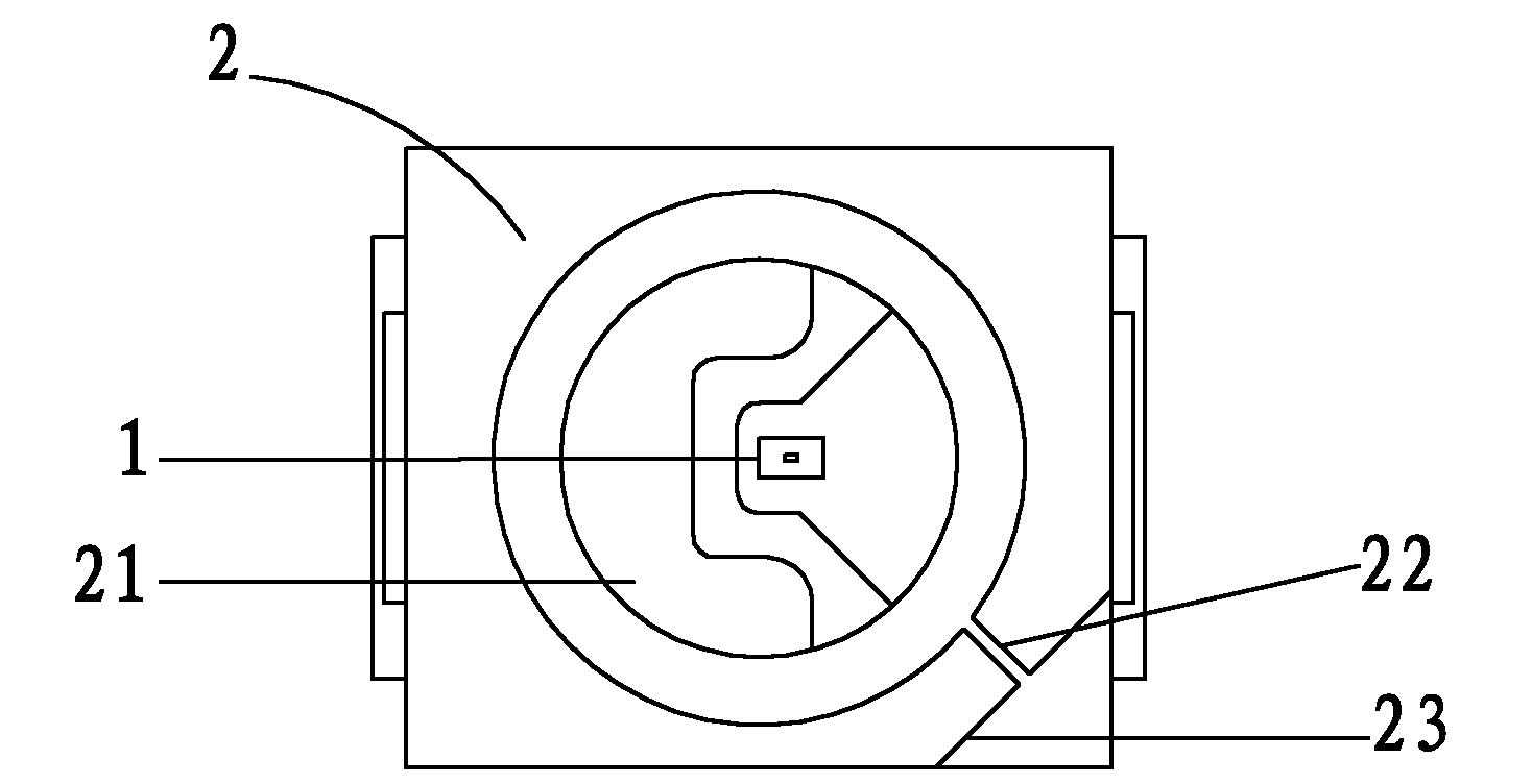
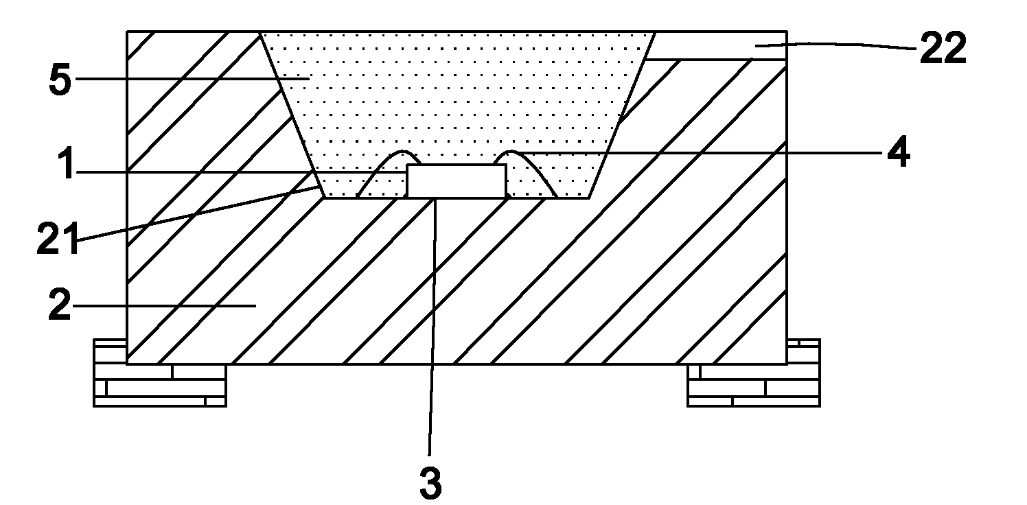
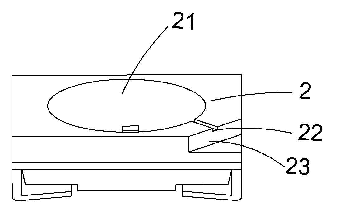
[0022] see figure 1 , figure 2 and image 3 , The LED of the present invention includes an LED blue light chip 1 and a socket 2 carrying the LED blue light chip 1 . The receiving base 2 has a concave groove 21 . The LED blue light chip 1 is fixed in the concave groove 21 by a chemical die-bonding glue 3. In this embodiment, the die-bonding glue 3 is silver glue or insulating glue. In the concave groove 21, the surface of the LED blue light chip 1 is provided with an external sealant 5, and the surface of the receiving seat 2 is provided with a glue overflow groove 22 that communicates the concave groove 21 with the outside world. The depth of the glue groove 22 is 1 / 8-1 / 6 of the depth of the concave groove 21 .

[0023] The LED of th...


PUM


Abstract

The invention discloses a light emitting diode (LED) and an encapsulating method thereof. The method comprises the following steps: providing a stacker with a groove and an LED blue light wafer, depositing or evaporating metal or alloy on the bottom of the blue light wafer, fixing the LED blue light wafer with metal or alloy deposited or evaporated on the bottom in the groove by solid crystal adhesive, and opening a rubber overflow groove leading the groove to be communicated with the outside on the surface of the stacker; electrically connecting negative and positive electrodes of the LED blue light wafer with negative and positive electrodes of the stacker respectively by lead wires; and encapsulating and molding the surface of the LED blue light wafer in the groove by external seal adhesive. By opening the rubber overflow groove on the surface of the stacker, residual external seal adhesive can flow to the outside of the groove through the rubber overflow groove when the external seal adhesive is used for encapsulation, and a horizontal plane is formed in the whole groove, so the light emitted by the LED blue light wafer can be radiated uniformly through the rubber on the horizontal plane, and the light emitting uniformity of the whole LED is consistent.

Description

technical field [0001] The invention relates to a lamp, in particular to an LED and a packaging method thereof. Background technique [0002] As a new type of light source, white LED is widely used in buildings, solar street lights, flashlights, car lights, table lamps, backlights, spotlights, gardens, etc. , wall lamps, small area decorative lighting for home and commercial lighting integrating decoration and advertising. [0003] Chinese patent application No. 200910109512.0 discloses an LED lamp and a packaging method, including an LED chip and a socket for carrying the LED chip. The surface of the LED chip is also packaged with a layer of sealing glue (not shown in the figure). [0004] However, the thickness of the above-mentioned outer sealant (not shown) applied on the surface of the LED chip is inconsistent, that is, the space above the height of the fixed LED chip in the metal cup is different from the space above the height of the unfixed LED chip, so the outer se...

Claims


Application Information

Patent Timeline
Patent Type & Authority Applications(China)
IPC IPC(8): H01L33/52H01L33/48
CPCH01L2224/45124H01L2224/45139H01L2224/45144H01L2224/45147H01L2224/48091H01L2924/00014H01L2224/45015H01L2924/207
Inventor 李漫铁王绍芳周杰冯珍
Owner LEDMAN OPTOELECTRONICS
Why Eureka
Try Eureka