Beam processing apparatus, beam processing method, and beam processed substrate

A processing device and processing method technology, which are applied to metal processing equipment, removal of conductive materials by electric discharge method, and manufacturing tools, etc., can solve problems such as damage to the layer to be processed, eliminate obstacles, simplify the structure of focusing components, and realize processing. effect of time

Inactive Publication Date: 2011-02-16
MARUBUN
View PDF15 Cites 6 Cited by
  • Summary
  • Abstract
  • Description
  • Claims
  • Application Information

AI Technical Summary

Problems solved by technology

In this case, the layer to be processed is in contact with the upper surface of the table, so the layer to be processed may be damaged, or it may be affected by the table while processing (eg, temperature, laser reflection, etc.)

Method used


Image

  • Beam processing apparatus, beam processing method, and beam processed substrate
  • Beam processing apparatus, beam processing method, and beam processed substrate
  • Beam processing apparatus, beam processing method, and beam processed substrate

Examples


Embodiment Construction

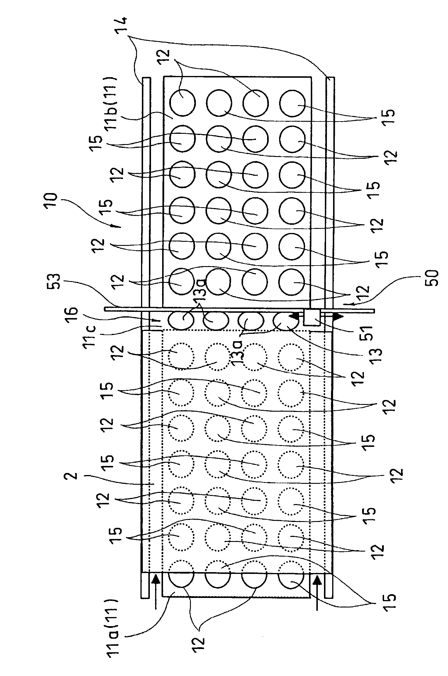
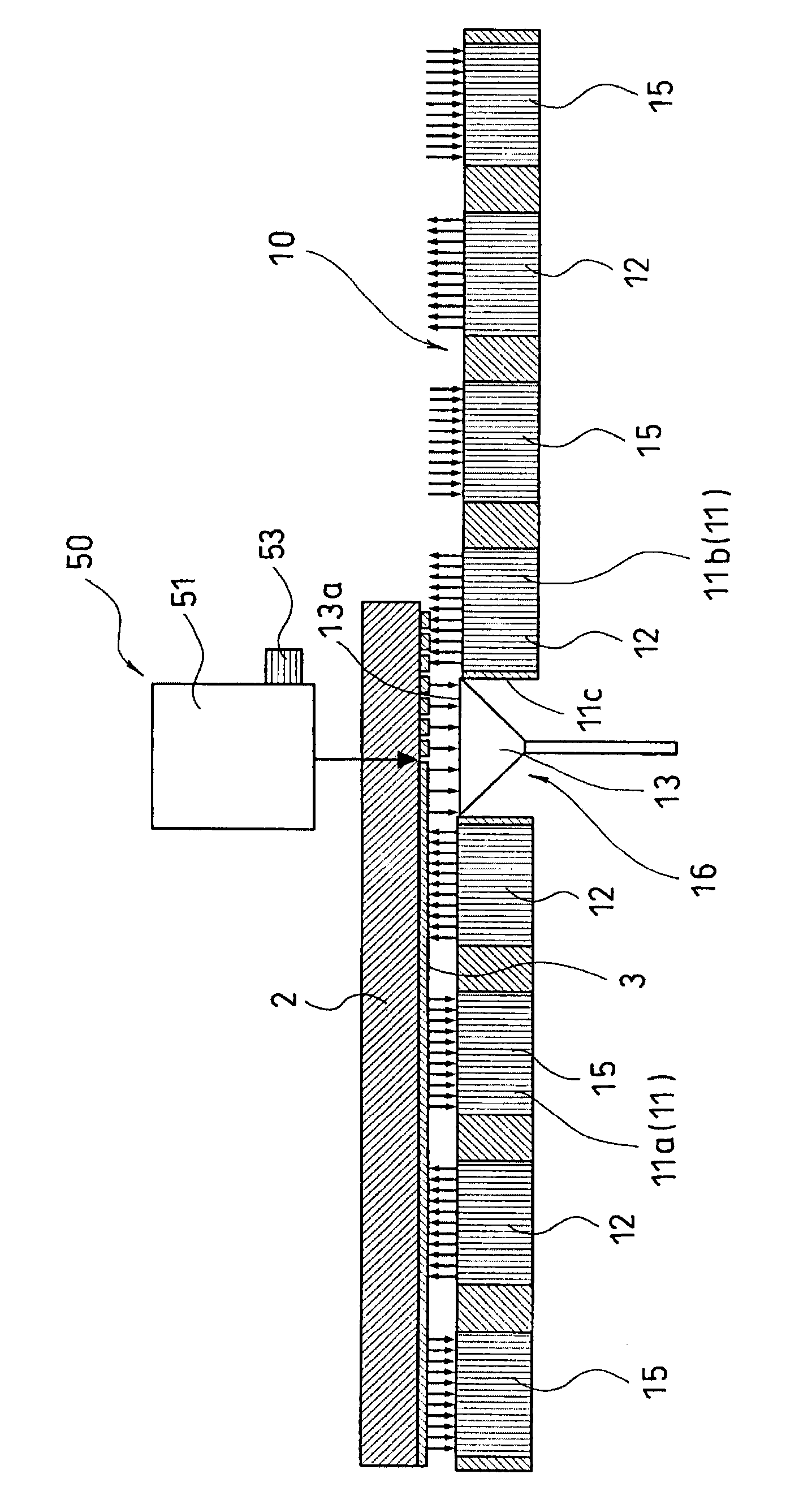
[0060] A first embodiment of the present invention will be described below with reference to the drawings.

[0061] figure 1 with figure 2 A schematic structure of the beam processing apparatus of the first embodiment of the present invention is shown.

[0062] The beam processing device in this example is suitable for, for example, manufacturing the above-mentioned power generation system, plasma display, etc., and can be used to pattern a thin film layer formed on a transparent substrate such as a glass substrate by using a beam (here, a laser beam) , in this patterning process, the thin film layer (layer to be processed) on the substrate is sublimated, liquefied, and peeled off by irradiating a laser beam to form grooves to bring the thin film layer into a divided state, whereby the thin film layer The thin film layer is formed into an arbitrary shape. Here, however, grooves are formed in the film so as to form, for example, a stripe shape or a matrix shape.

[0063] T...


PUM

PropertyMeasurementUnit
wavelengthaaaaaaaaaa

Abstract

Disclosed is a beam processing apparatus that processes a layer to be processed (3) formed on one surface of a substrate (2), by irradiating the same with a beam. The beam processing apparatus comprises: a gas floating mechanism (10) that emits gas to support the substrate so as to float in a flat position; and a beam irradiating means (50) that processes the layer to be processed (3), formed on one surface of the substrate (2), by irradiating the same with a beam. The substrate (2) is arranged above the gas floating mechanism (10) so that the layer to be processed (3) formed on one surface of the substrate (2) is facing downwards. Processing is carried out on the layer to be processed (3) by emitting a beam through the substrate (2) and onto the layer to be processed (3) using the beam irradiating means (50) from above the other side of the substrate (2).

Description

technical field [0001] The present invention relates to a beam processing device, a beam processing method, and a beam processed substrate having a layer (thin film) to be processed that has been processed by the above beam processing device. The beam processing apparatus, the beam processing method, and the beam processed substrate can be suitably used in the case where a semiconductor device serving as a power generation system using, for example, the photoelectric effect is formed on a substrate such as a glass substrate, and the beam (laser, etc.) Thin film patterning for forming semiconductor devices. Background technique [0002] Usually, in the manufacturing process of the above-mentioned power generation system using the silicon-based amorphous film, a transparent electrode (such as indium oxide, tin oxide, zinc oxide, etc.) layer is first patterned on a large glass substrate, and then, on the glass substrate An amorphous silicon layer (photoelectric conversion laye...

Claims


Application Information

Patent Timeline
Patent Type & Authority Applications(China)
IPC IPC(8): B23K26/42H05K3/08B23K26/00B23K26/10H05K3/00B23K26/14B23K26/16B23K26/364H01L21/28H01L21/768
CPCH05K2203/081H05K3/027H05K2203/0165B23K26/10B23K26/0876H05K2203/1581H05K2201/0108
Inventor 仲田悟基山冈裕木野本亮
Owner MARUBUN
Why Eureka
Try Eureka