Semiconductor memory and method for manufacturing the same

A semiconductor and memory technology, applied in the field of semiconductor memory and its manufacturing, can solve the problems of increasing the number of manufacturing steps, increasing manufacturing costs, ensuring the reliability and fast operation of non-volatile memory, and achieving the effect of increasing bit density

Inactive Publication Date: 2011-02-23
KK TOSHIBA
View PDF8 Cites 19 Cited by
  • Summary
  • Abstract
  • Description
  • Claims
  • Application Information

AI Technical Summary

Problems solved by technology

[0006] (2) The short-channel effect and the narrow-channel effect become prominent rapidly due to the device size reduction accompanying the scaling down, which makes it difficult to ensure the reliability and fast operation of the nonvolatile memory generation by generation
Therefore, an increase in the number of memory layers leads to an increase in the number of manufacturing steps, and also leads to an increase in manufacturing cost
As a result, this technology has the problem of manufacturing cost per bit

Method used


Image

  • Semiconductor memory and method for manufacturing the same
  • Semiconductor memory and method for manufacturing the same
  • Semiconductor memory and method for manufacturing the same

Examples


Embodiment Construction

[0123] Embodiments of the present invention will be described below with reference to the drawings.

[0124] First, a first embodiment of the present invention will be described.

[0125] This embodiment relates to a semiconductor memory, and more specifically, to a nonvolatile semiconductor memory.

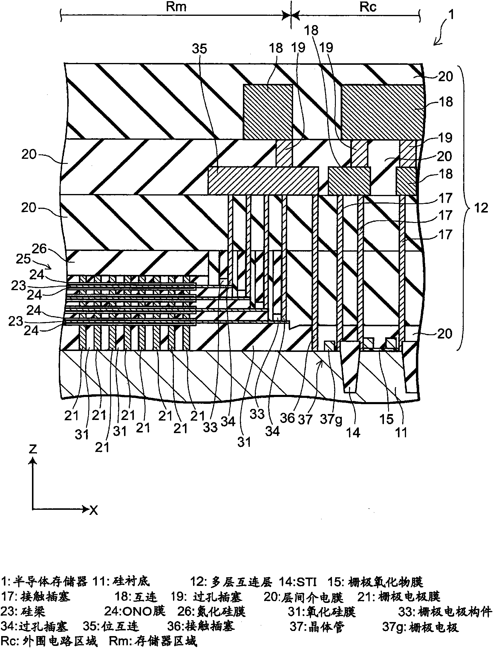
[0126] figure 1 A cross-sectional view parallel to the extending direction of a silicon beam is shown to illustrate the semiconductor memory according to this embodiment.

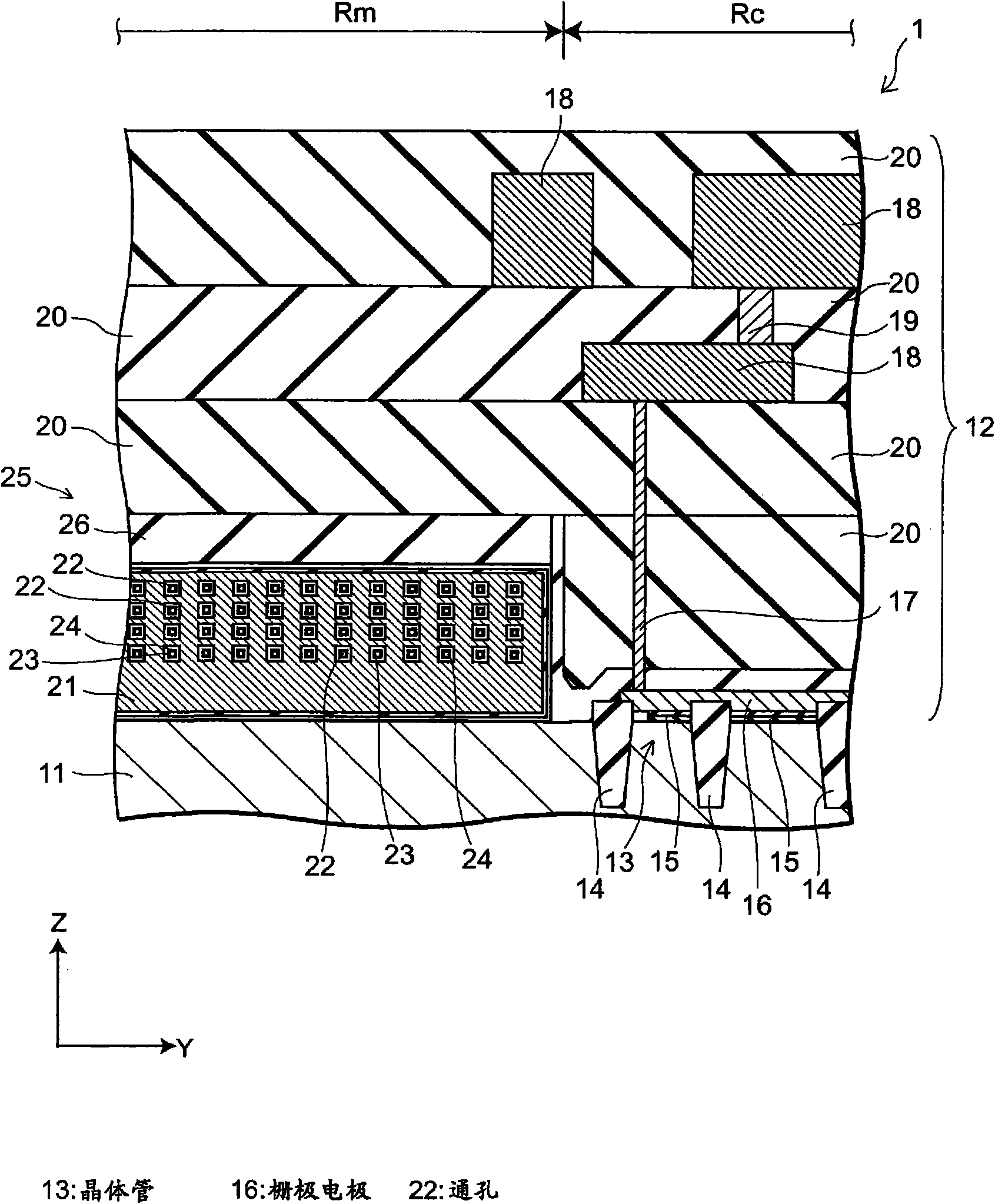
[0127] figure 2 A cross-sectional view perpendicular to the extending direction of the silicon beams of the semiconductor memory according to this embodiment is illustrated.

[0128] image 3 To illustrate a cross-sectional view of the inside of the memory region of the semiconductor memory according to this embodiment.

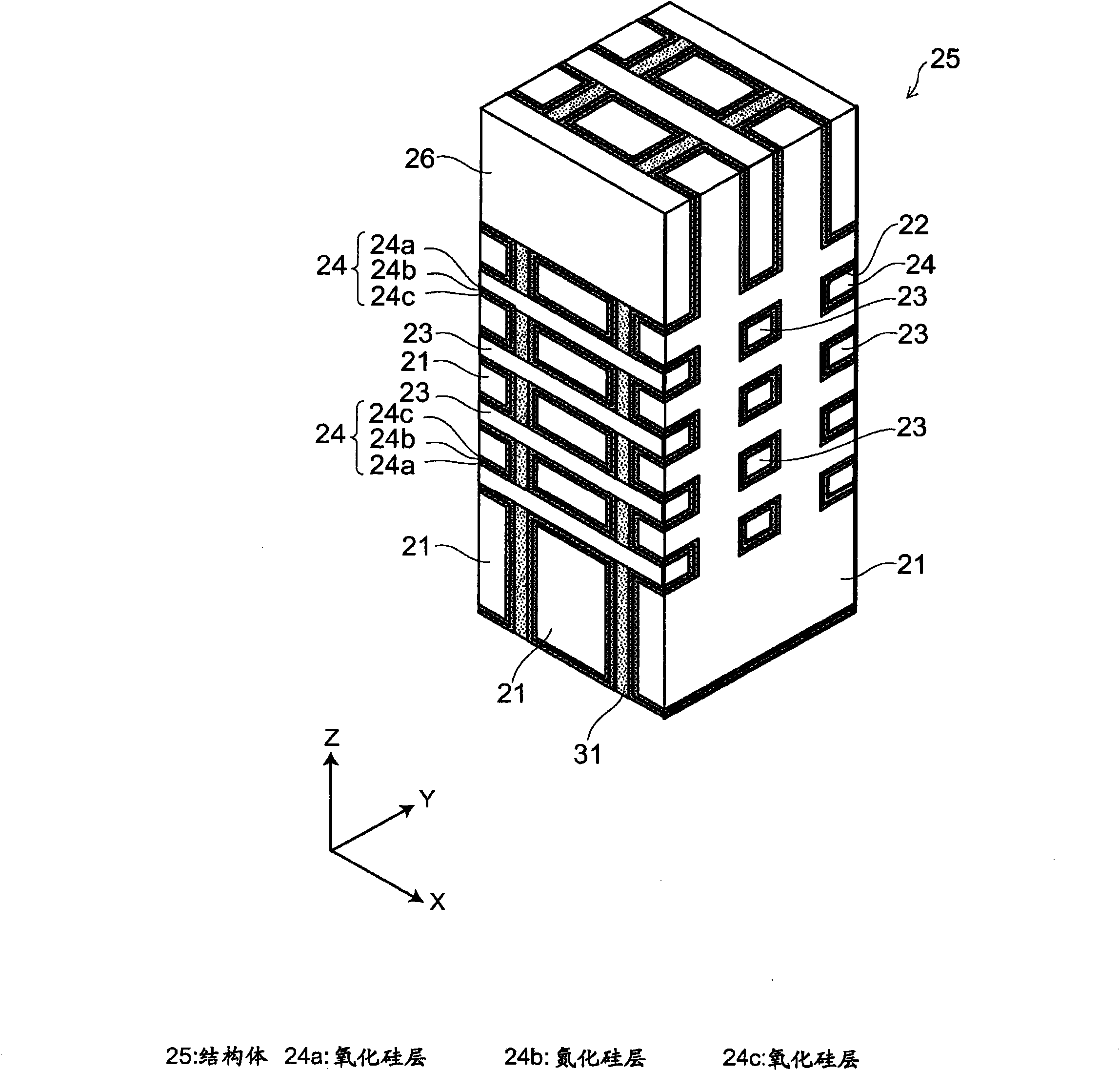
[0129] Figure 4A perspective view illustrating the gate electrode film and silicon beams in the memory region of the semiconductor memory according to this embodiment.

[0130] Fig...


PUM


Abstract

Provided are a semiconductor memory wherein bit density is improved by three-dimensionally arranging cells, and a method for manufacturing such semiconductor memory. In a semiconductor memory (1), a plurality of gate electrode films (21) are arranged on a silicon substrate (11). Gate electrode films (21) are arranged along one direction (X direction) parallel to the upper surface of the silicon substrate (11). Each gate electrode film (21) has a shape of a grid-like board, and a plurality of through holes (22) are formed in matrix when viewed from the X direction. Furthermore, a plurality of silicon beams (23) are arranged such that the beams penetrate the through holes (22) on the gate electrode films (21) and extend in the X direction. Furthermore, an ONO film (24), including a charge accumulating layer, is arranged between the gate electrode film (21) and the silicon beam (23).

Description

technical field [0001] The present invention relates to a semiconductor memory and a method of manufacturing the same, and more particularly, to a semiconductor memory including three-dimensionally arranged memory cells and a method of manufacturing the same. Background technique [0002] Flash memory is widely used as high-capacity data storage in cellular phones, digital cameras, USB (Universal Serial Bus) memory, silicon audio players, etc. The cost is reduced and the market continues to expand. In addition, new applications are rapidly emerging, enabling a virtuous cycle in which scaling down and lower manufacturing costs find new markets. [0003] In particular, NAND flash memory allows a plurality of active areas (hereinafter also referred to as "AA") to share a gate conductor (hereinafter also referred to as "GC"), thereby substantially realizing a 4F 2 The intersection primitive with a primitive area of ​​, where F is the minimum processing size, is being rapidly s...

Claims


Application Information

Patent Timeline
Patent Type & Authority Applications(China)
IPC IPC(8): H01L29/792H01L27/10H01L29/788H01L21/8247H01L27/115
CPCH01L27/11582H01L27/11565H01L27/11578H10B41/35H10B43/10H10B43/20H10B43/27H01L27/0688
Inventor 清利正弘
Owner KK TOSHIBA
Why Eureka
Try Eureka