Three-dimensional memory having four stacked layers

A memory, layer stacking technology, applied in the semiconductor field, can solve problems such as inability to provide bit density, competition, etc.

Pending Publication Date: 2021-01-26
YANGTZE ADVANCED MEMORY INDUSTRIAL INNOVATION CENTER CO LTD
View PDF0 Cites 1 Cited by
  • Summary
  • Abstract
  • Description
  • Claims
  • Application Information

AI Technical Summary

Problems solved by technology

However, the two-layer stacked memory cell architecture cannot provide sufficient bit density to compete with mainstream DRAM (Dynamic Random Access Memory) and NAND-type memories

Method used


Image

  • Three-dimensional memory having four stacked layers
  • Three-dimensional memory having four stacked layers
  • Three-dimensional memory having four stacked layers

Examples


Embodiment Construction

[0040] In order to make the technical solutions and advantages of the embodiments of the present invention more clear, the specific technical solutions of the invention will be further described in detail below in conjunction with the drawings in the embodiments of the present invention.

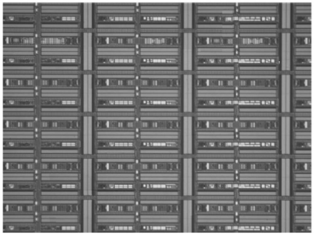
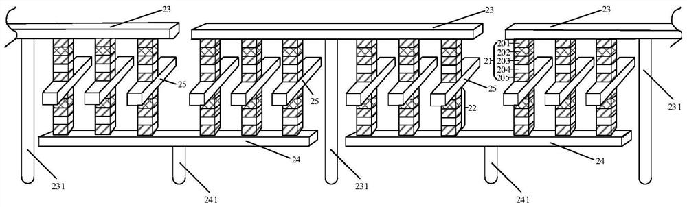
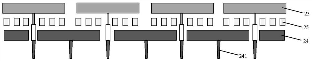
[0041] figure 1 It is a schematic diagram of a three-dimensional phase-change memory cell array observed by a scanning electron microscope. From figure 1 It can be seen that the three-dimensional phase change memory chip is composed of a plurality of small memory cell array blocks with a single bit line, word line and memory cells. A three-dimensional phase-change memory generally includes a top bit line, a word line, a bottom bit line, and a memory cell located at the intersection of the bit line and the word line. In practical application, the word line, top bit line and bottom bit line are usually formed by 20nm / 20nm constant line width (L / S, line / space) formed after the patterning proc...


PUM


Abstract

The embodiment of the invention provides a three-dimensional memory with four stacked layers. The three-dimensional memory comprises at least one memory cell array block; wherein the memory cell arrayblock comprises a first bit line layer, a second bit line layer and a third bit line layer which are sequentially arranged from top to bottom and are parallel to one another, and the bit lines of thebit line layers are parallel to each other, and the projections of the bit lines of the bit line layers on the first plane are partially overlapped; a first word line layer between the first bit linelayer and the second bit line layer; a second word line layer between the second bit line layer and the third bit line layer; wherein the word lines of each word line layer are parallel to each other, and the projection of the word line of each word line layer on the first plane is vertical to the projection of the bit line of the first bit line layer on the first plane; and four memory cell layers which are respectively positioned between two adjacent bit line layers and word line layers.

Description

technical field [0001] The invention relates to the technical field of semiconductors, in particular to a three-dimensional memory with four layers stacked. Background technique [0002] Phase Change Memory (PCM, Phase Change Memory) is a storage technology that uses chalcogenide as a storage medium, and uses the resistance difference of materials in different states to store data. PCM has the advantages of bit-addressable, no data loss after power failure, high storage density, and fast read and write speed, and is considered to be the most promising next-generation memory. [0003] In the related art, the architecture of the mainstream three-dimensional phase change memory includes two layers of stacked memory cells. However, the two-layer stacked memory cell architecture cannot provide sufficient bit density to compete with mainstream DRAM (Dynamic Random Access Memory) and NAND memory. In order to improve the competitiveness of 3D phase change memory, it is necessary t...

Claims


Application Information

Patent Timeline
Patent Type & Authority Applications(China)
IPC IPC(8): H01L27/24G11C13/00
CPCG11C13/0004G11C13/0026G11C13/0028H10B63/32
Inventor 刘峻
Owner YANGTZE ADVANCED MEMORY INDUSTRIAL INNOVATION CENTER CO LTD
Why Eureka
Try Eureka