Method and Structure for Integrated High Density Memory Device

a memory device and high density technology, applied in the field of high density memory device manufacturing, can solve the problems of high manufacturing cost per bit of solid state memory device and difficult density scaling, and achieve the effects of high mechanical bandwidth, improved reliability, and improved power efficiency

Inactive Publication Date: 2007-05-03
YANG XIAO
View PDF8 Cites 3 Cited by
  • Summary
  • Abstract
  • Description
  • Claims
  • Application Information

AI Technical Summary

Benefits of technology

[0007] Many benefits are achieved by way of the present invention over conventional techniques. For example, the present technique provides an easy to use process that relies upon conventional technology. In some embodiments, the method provides for an integrated drive storage device based on electrostatic actuation are more power efficient than conventional HDD with magnetic actuation. In other embodiments, the method provides for the integrated disk storage device to have higher mechanical bandwidth than conventional HDD, which yields fast access speed and short R / W cycle time. Furthermore, the integrated disk storage device is fabricated on a semiconductor substrate which has higher bit density and scalability than conventional HDD. Additionally, the method provides a process that is compatible with conventional semiconductor and MEMS fabrication process technology without substantial modifications to conventional equipment and processes. Preferably, the invention provides for an integrated disk storage device including Integrated Circuits and sensing elements for various applications.

Problems solved by technology

However, comparing to HDD, solid state memory devices have higher manufacturing cost per bit and are difficult to scale in density.

Method used


Image

  • Method and Structure for Integrated High Density Memory Device
  • Method and Structure for Integrated High Density Memory Device
  • Method and Structure for Integrated High Density Memory Device

Examples


Embodiment Construction

[0016] According to the present invention, techniques for manufacturing objects are provided. More particularly, the invention provides a method and device for fabricating high density memory device.

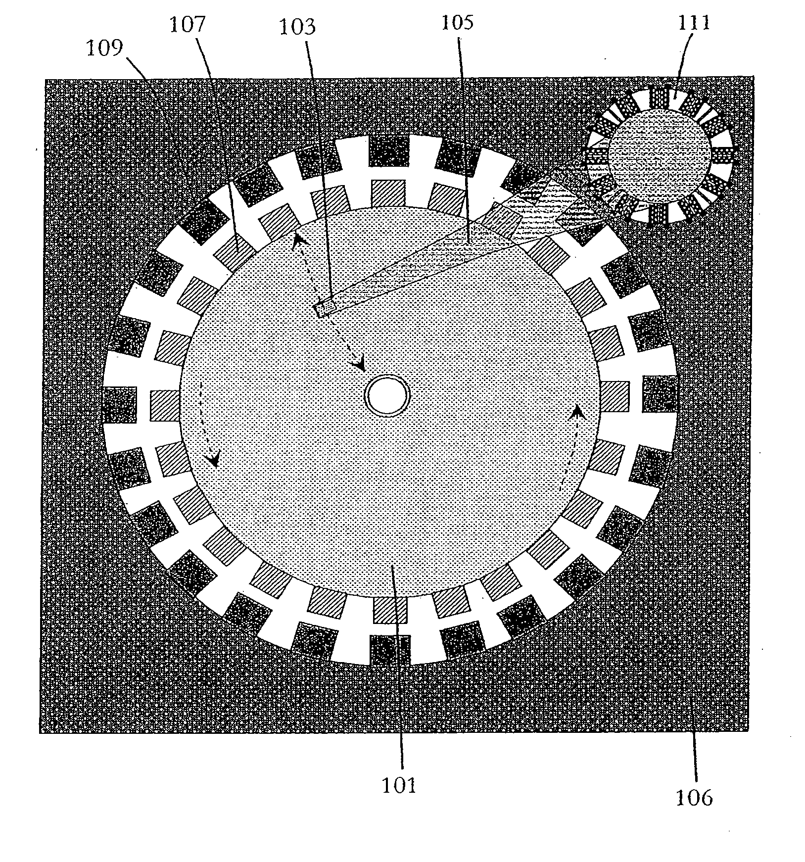
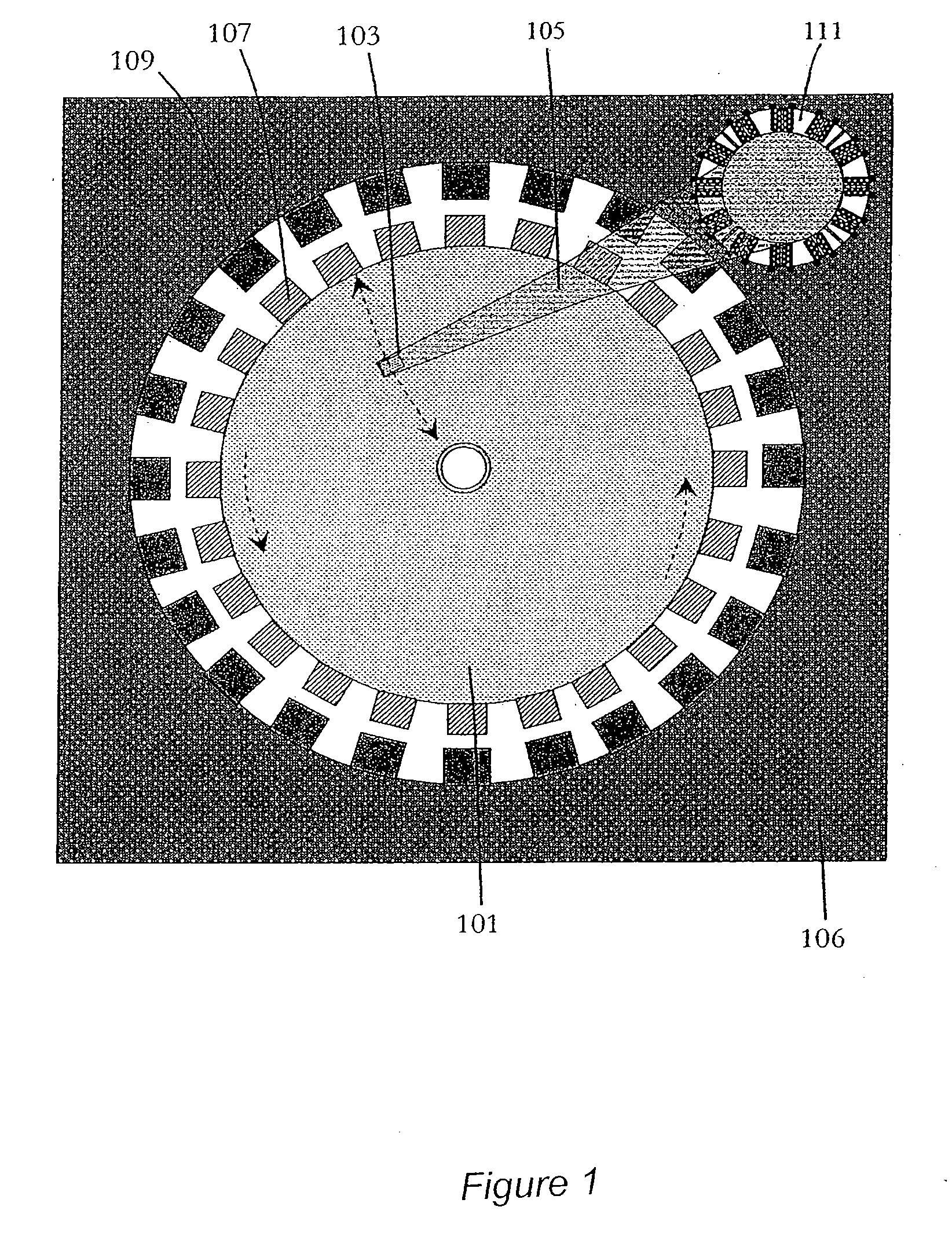
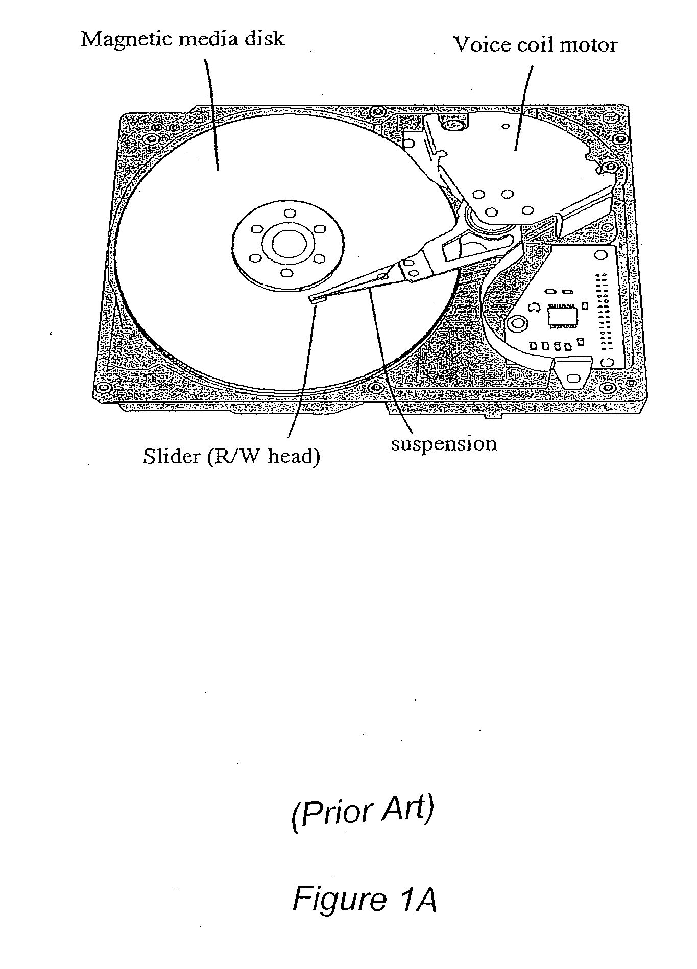
[0017]FIG. 1 is a simplified top-view diagram illustrating components of an integrated storage device according to one embodiment of the present invention. As illustrated, the integrated memory device is consisted with a rotating media plate 101 and a Read / Write (R / W) head 103 on a movable suspension 105, similar to a Hard Disk Drive (HDD). Unlike HDD, the media plate is micro fabricated on a substrate 106. Both the plate and head suspension are actuated by electrostatic forces instead of magnetic forces used in HDD. The media plate is also the rotor and has a plurality of ‘teeth’ electrodes 107 that have corresponding stator electrodes 109. The head suspension is micro fabricated and anchored to a comb drive actuator which is also micro fabricated. The R / W head can be based on one of f...


PUM

PropertyMeasurementUnit
diameteraaaaaaaaaa
magnetoresistiveaaaaaaaaaa
near field scanning optical microscopeaaaaaaaaaa

Abstract

The present invention provides a method and device for fabricating high density memory device. Similar to a Hard Disk Drive (HDD), the integrated memory device is consisted with a rotating media plate and a Read/Write (R/W) head on a movable suspension. Unlike HDD where the media plate is coupled to a motor, the media plate is micro fabricated on a semiconductor substrate and is also a motor which is actuated and rotated by electrostatic forces. The head suspension is also micro fabricated and anchored to an electrostatic comb drive micro actuator. Control IC can also be integrated on-chip with the integrated memory device as well as acceleration sensing devices such as MEMS accelerator for anti-shock measures. The integrated disk storage device is fabricated by conventional semiconductor and MEMS fabrication process technology.

Description

CROSS-REFERENCES TO RELATED APPLICATIONS [0001] This application claims priority to provisional application Ser. No. 60 / 732,448; filed on Oct. 31, 2005; commonly assigned, and of which is hereby incorporated by reference for all purposes.BACKGROUND OF THE INVENTION [0002] This present invention relates to a method and structure for fabricating a high density memory device. Hard Disk Drive (HDD) and solid state memory devices such as flash are two main storage devices. Solid state memory devices have fast Read / Write (R / W) speed, small form factor, and low power consumption. However, comparing to HDD, solid state memory devices have higher manufacturing cost per bit and are difficult to scale in density. [0003] Thus, there is a need in the art for methods and apparatus for fabricating a memory device that has fast R / W speed, small form factor, low cost, high density, low power consumption and scalable. SUMMARY OF THE INVENTION [0004] According to the present invention, techniques for ...

Claims


Application Information

Patent Timeline
Patent Type & Authority Applications(United States)
IPC IPC(8): G11B5/48
CPCB82Y10/00G11B5/4886G11B7/08576G11B9/1454
Inventor YANG XIAO (CHARLES)
Owner YANG XIAO
Why Eureka
Try Eureka