Formation method of memory device

A storage device and device layer technology, which is applied in the manufacture of electrical solid-state devices, semiconductor devices, semiconductor/solid-state devices, etc., can solve the problems of large space area, achieve the effect of reducing space area, reducing bit cost, and increasing bit density

Active Publication Date: 2016-07-13
SEMICON MFG INT (SHANGHAI) CORP
View PDF5 Cites 2 Cited by
  • Summary
  • Abstract
  • Description
  • Claims
  • Application Information

AI Technical Summary

Problems solved by technology

[0005] However, the space occupied by the existing 3D NAND gate flash storage unit is still relatively large, and it is necessary to further reduce the space utilization of the 3D NAND flash memory storage unit, further increase the bit density, and reduce the bit cost.

Method used


Image

  • Formation method of memory device
  • Formation method of memory device
  • Formation method of memory device

Examples


Embodiment Construction

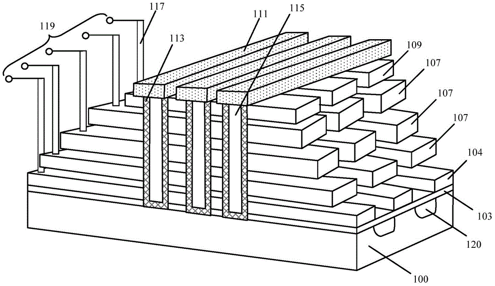
[0034] As mentioned in the background art, the existing three-dimensional NAND gate flash memory storage unit still occupies a relatively large space area.

[0035] Please continue to refer figure 1 The pattern size of the overlapping control gates 107 projected on the surface of the substrate 100 decreases layer by layer from bottom to top, so that each control gate layer 107 can expose part of the control gate layer of the next layer, so that it can be used in each layer. A word line plug 117 is formed on the surface of the layer control gate layer 107 , and the word line plug 117 is only connected to one layer of the control gate layer 107 and does not contact with several other layers of control gate layers 107 .

[0036]After research, it is found that a process for forming a flash storage unit of a three-dimensional NAND gate in an embodiment of the present invention includes: providing a substrate; forming several overlapping composite layers on the surface of the subst...


PUM

PropertyMeasurementUnit
thicknessaaaaaaaaaa
thicknessaaaaaaaaaa
thicknessaaaaaaaaaa

Abstract

The invention relates to a formation method of a memory device. The method includes the following steps that: a multi-layer overlapped composite layer is formed on the surface of a substrate, the surface of the composite layer is provided with a mask layer, the composite layers include insulating layers and device layers arranged on the surfaces of the insulating layers; a strengthened layer is formed on a part of the side wall surface of the mask layer, and the strengthened layer exposes the top surface and a part of the side wall surface of the mask layer; with the strengthened layer adopted as a mask, the exposed side wall surface of the mask layer is etched, so that a part of the surface of the composite layer at the top is exposed; with the mask layer and the strengthened layer adopted as a mask, the exposed composite layer is etched, the etching thickness of the composite layer is greater than or equal to the thickness of a single device layer; the steps in which the side wall of the mask layer and the composite layer are etched are repeated for once or by a plurality of times until the size of the projection pattern of the plurality of device layers is gradually decreased from the bottom layer to the top layer along at least one direction, so that the plurality of device layers can form a steeped structure which is shrunk gradually from the bottom layer to the top layer. The memory device formed by the method of the invention has the advantages of low space occupancy rate, high bit density and low bit cost.

Description

technical field [0001] The present invention relates to the technical field of semiconductor manufacturing, in particular to a method for forming a storage device Background technique [0002] In recent years, the development of flash memory (flash memory) memory is particularly rapid. The main feature of flash memory is that it can keep stored information for a long time without power on, and has the advantages of high integration, fast access speed, easy erasing and rewriting, etc. Has been widely used. In order to further increase the bit density of the flash memory while reducing the bit cost, a three-dimensional NAND (3D NAND) flash memory is proposed. [0003] Please refer to figure 1 , figure 1 It is a structural schematic diagram of an existing three-dimensional NAND gate flash storage unit, including: a substrate 100; an isolation layer 103 located on the surface of the substrate 100; a bottom selection gate 104 located on the surface of the isolation layer 103;...

Claims


Application Information

Patent Timeline
Patent Type & Authority Applications(China)
IPC IPC(8): H01L21/8247H01L27/11563
Inventor 何其暘孟晓莹
Owner SEMICON MFG INT (SHANGHAI) CORP
Why Eureka
Try Eureka