Matrix MOV circuit board structure and manufacturing method thereof

A circuit board and matrix technology, which is applied in the field of matrix MOV circuit board structure and its manufacturing, can solve the problems of single suppression component breakdown, etc., to solve the problems that are difficult to withstand high current impact, break through the impact current resistance, and reduce contact resistance. Effect

Inactive Publication Date: 2011-03-30
DELTA GREENTECH CHINA CO LTD
View PDF0 Cites 9 Cited by
  • Summary
  • Abstract
  • Description
  • Claims
  • Application Information

AI Technical Summary

Problems solved by technology

For the impact of high current, a single suppression element is likely to be broken down

Method used


Image

  • Matrix MOV circuit board structure and manufacturing method thereof
  • Matrix MOV circuit board structure and manufacturing method thereof

Examples


specific Embodiment

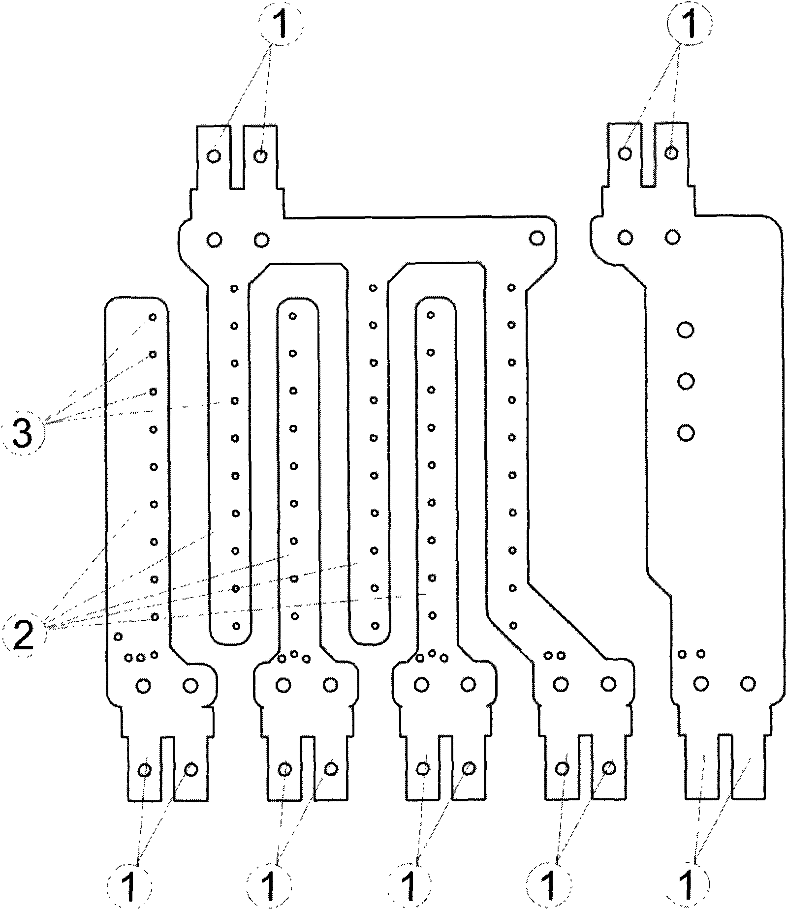
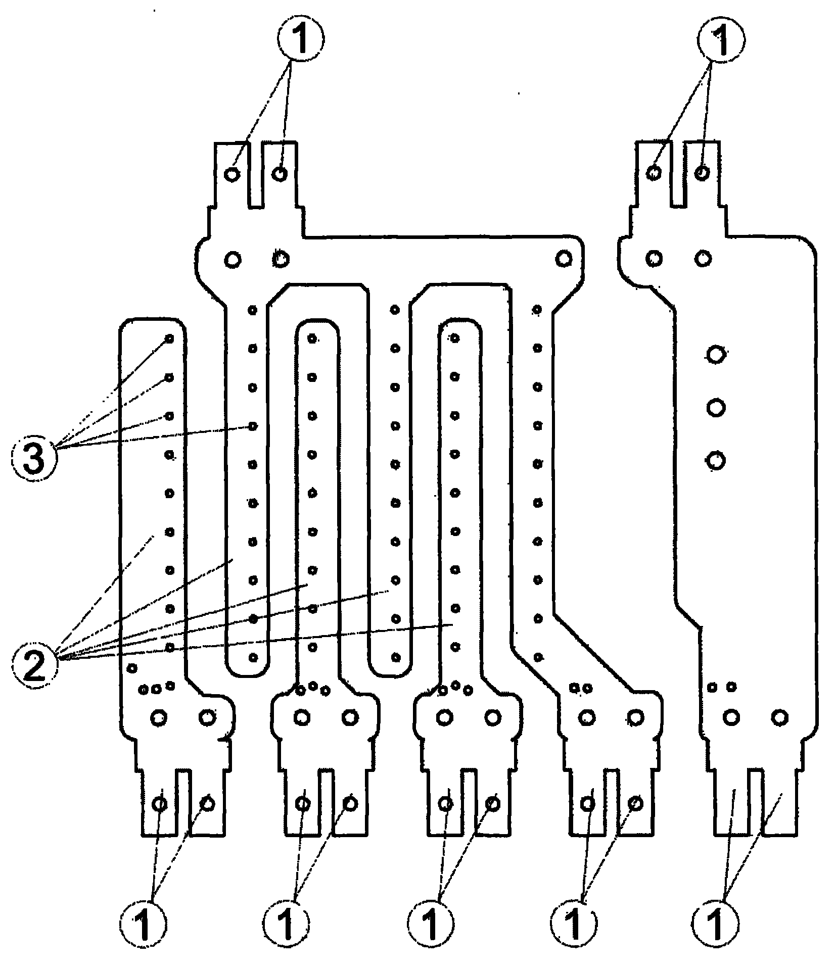
[0031] A circuit board structure of a matrix MOV, which comprises a PCB printed circuit board, a copper conductive busbar, and a plastic module in which the MOV is combined with a thermal fuse and a sampling resistor; the copper conductive busbar is attached to the PCB printed circuit on the copper foil of the board; the plastic module that combines the MOV with the thermal fuse and the sampling resistor is directly welded on the conductive bus bar.

[0032] Please see figure 1 , the copper conductive busbar includes: a copper bar 2 and an electrode 1 for connecting to a dual-port terminal, and is provided with a component pin welding hole 3 . The PCB printed circuit board is provided with component pin welding holes, and the component pin welding holes 3 on the copper conductive busbar correspond to the position of the component pin welding holes on the PCB printed circuit board, so that the copper The conductive busbar is synchronized with the PCB printed circuit board.

...


PUM


Abstract

The invention discloses a matrix metal oxide varistor (MOV) circuit board structure and a manufacturing method thereof. The structure comprises a printed circuit board (PCB), a copper conductive busbar, and MOV, thermal fuse body and sampling resistor-combined plastic modules, wherein the copper conductive busbar is attached to a copper foil of the PCB; the copper conductive busbar is integrated with an electrode used for connecting a dual-port wiring terminal into a whole and is provided with an element pin welding hole which is synchronous with the PCB; and the MOV, thermal fuse body and sampling resistor-combined plastic module is directly welded on the conductive busbar. In the circuit board structure, the integrally punched copper conductive busbar is adopted and attached to the copper foil of the PCB, the sectional area of a lead of the circuit board is increased, and the contact resistance is reduced. Therefore, the capacity of the circuit board of bearing heavy current is improved, and the equalized current between the matrix distribution MOV, thermal fuse body and sampling resistor-combined plastic modules is realized.

Description

technical field [0001] The invention relates to a PCB copper foil current expansion technology and a matrix MOV current sharing technology in the field of lightning protection, in particular to a matrix MOV circuit board structure and a manufacturing method thereof. Background technique [0002] The design of PCB printed circuit boards in lightning protection products is widely used at home and abroad, but it is limited by the thickness of the copper foil of the PCB board, so that when the lightning protection product passes a relatively large impact current, such as above 100kA, the copper foil of the PCB board will be damaged. Melted by the instantaneous high current, causing the copper foil to vaporize, making the SPD invalid. [0003] The industry also adopts remedial measures to weld (tin solder) copper wires on the surface of copper foil in order to expand the current carrying capacity. However, in fact, this method cannot perfectly solve the impact of high current, b...

Claims


Application Information

Patent Timeline
Patent Type & Authority Applications(China)
IPC IPC(8): H05K1/18H05K3/34H02H9/04
Inventor 李文富刘韧
Owner DELTA GREENTECH CHINA CO LTD
Why Eureka
Try Eureka