Demodulator circuit for the UHF (Ultrahigh Frequency) radio frequency identification label chip

A technology of radio frequency identification tags and demodulation circuits, which is applied to record carriers used in machines, instruments, computer components, etc., can solve the problem of small dynamic range and achieve the effect of large input dynamic range

Active Publication Date: 2012-05-30
四川电子科技大学教育发展基金会
View PDF0 Cites 0 Cited by
  • Summary
  • Abstract
  • Description
  • Claims
  • Application Information

AI Technical Summary

Problems solved by technology

[0006] The purpose of the present invention is to overcome the shortcoming of a relatively small dynamic range brought about by using a grounded MOS transistor instead of a high-value resistor, and propose a demodulation circuit for an ultra-high frequency radio frequency identification tag chip

Method used


Image

  • Demodulator circuit for the UHF (Ultrahigh Frequency) radio frequency identification label chip
  • Demodulator circuit for the UHF (Ultrahigh Frequency) radio frequency identification label chip
  • Demodulator circuit for the UHF (Ultrahigh Frequency) radio frequency identification label chip

Examples


Embodiment 1

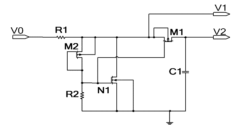
[0020] Embodiment one: if figure 1 As shown, the demodulation circuit for the UHF RFID tag chip includes an overvoltage protection circuit and an average generating circuit. The overvoltage protection circuit is composed of the first resistor R1, the second resistor R2, the second PMOS transistor M2 and the first NMOS transistor N1; the average generating circuit is composed of the first PMOS transistor M1 and the first capacitor C1, which is used to generate the envelope signal The source of the first PMOS transistor M1 is connected to the drain of the first NMOS transistor N1 in the overvoltage protection circuit; the gate of the first PMOS transistor M1 is connected to the first NMOS transistor N1 in the overvoltage protection circuit. The gates of the NMOS transistor N1 are connected; the drain of the first PMOS transistor M1 is connected to the ground through the first capacitor C1 as the output terminal of the average generating circuit.

[0021] In the overvoltage prot...

Embodiment 2

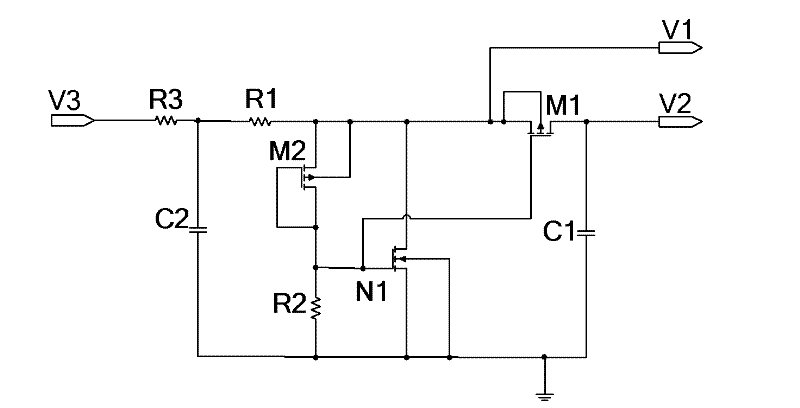
[0023] Embodiment two: if figure 2 As shown, on the basis of the first embodiment, the demodulation circuit for the UHF radio frequency identification tag chip also includes a low-pass filter circuit. The low-pass filter circuit is composed of a second capacitor C2 and a third resistor R3, one end of the third resistor R3 is grounded through the second capacitor C2, and is connected to the input end of the overvoltage protection circuit as the output end of the low-pass filter circuit, The other end of the third resistor R3 serves as the input end of the low-pass filter circuit to input the envelope signal.

[0024] The envelope signal V3 passes through a low-pass filter circuit and an overvoltage protection circuit to generate an envelope signal V1 after overvoltage protection, and then passes through an average value generating circuit to generate an envelope average value signal V2.

Embodiment 3

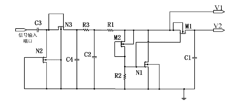
[0025] Embodiment three: as image 3 As shown, on the basis of the second embodiment, the demodulation circuit for the UHF radio frequency identification tag chip also includes an envelope detection circuit. The envelope detection circuit is composed of a third capacitor C3, a fourth capacitor C4, a second NMOS transistor N2 and a third NMOS transistor N3, the third capacitor C3 is connected to a signal input port; the second NMOS transistor N2 The source of the second NMOS transistor N2 is connected to the signal input port through the third capacitor C3; the gate and drain of the second NMOS transistor N2 are connected and connected to the ground; the gate and drain of the third NMOS transistor N3 are connected to the second The source of the NMOS transistor N2; the source of the third NMOS transistor N3 is connected to the input terminal of the low-pass filter circuit and connected to the ground through the fourth capacitor C4.

[0026] The signal received by the signal in...


PUM


Abstract

The invention discloses a demodulator circuit for a UHF (Ultrahigh Frequency) radio frequency identification label chip. Aiming at the defect of smaller dynamic range brought by the substitution of a traditional grid-grounded MOS (Metal-Oxide Semiconductor) tube for a high-resistance resistor, the invention provides a demodulator circuit which comprises an overvoltage protection circuit and a mean value generating circuit. The demodulator circuit connects the grid of a first PMOS (P-Channel Metal Oxide Semiconductor) tube in the mean value generating circuit with the grid of a first NMOS (N-Channel Metal Oxide Semiconductor) tube in the overvoltage protection circuit, and the grid level of the first PMOS tube automatically varies with the source level thereof by the partial pressure action of a second PMOS tube and a second resistor when the source level of the first PMOS tube rises or falls so that the absolute values of a grid voltage and a source voltage of the first PMOS tube are kept stable, the first PMOS tube has stable equivalent resistance in a large dynamic range, and the demodulator circuit of the invention has greater dynamic input range compared with the traditional demodulator circuit.

Description

technical field [0001] The invention belongs to the technical field of radio frequency identification, and in particular relates to a demodulation circuit for an ultra-high frequency radio frequency identification tag chip. Background technique [0002] Radio Frequency Identification (RFID, Radio Frequency Identification) technology is the use of radio frequency for long-distance communication to achieve the purpose of item identification, can be used to track and manage almost all physical objects, in industrial automation, commercial automation, transportation control management, anti-counterfeiting, etc. It has broad application prospects in many fields, even military use, and has attracted widespread attention at present. [0003] Passive UHF electronic tags have the characteristics of long range and low cost. The chip of a typical passive UHF electronic tag includes three main parts, which are RF analog front end, digital baseband processor and multi-time programming (...

Claims


Application Information

Patent Timeline
Patent Type & Authority Patents(China)
IPC IPC(8): G06K19/077
Inventor 王耀文光俊
Owner 四川电子科技大学教育发展基金会
Why Eureka
Try Eureka