Supercharge Your Innovation With Domain-Expert AI Agents!

Liquid crystal display and manufacturing method thereof

A technology of liquid crystal display and manufacturing method, which is applied in semiconductor/solid-state device manufacturing, instruments, optics, etc., can solve the problems of pixel display grayscale difference and affect the screen display quality, etc., to eliminate the display grayscale difference of each pixel and improve the display. quality effect

Active Publication Date: 2011-04-20
BOE TECH GRP CO LTD +1
View PDF0 Cites 16 Cited by
  • Summary
  • Abstract
  • Description
  • Claims
  • Application Information

AI Technical Summary

Problems solved by technology

According to the feedthrough calculation formula, the size of the pixel electrode feedthrough is proportional to the parasitic capacitance and inversely proportional to the sum of the parasitic capacitance, storage capacitance and liquid crystal capacitance. Therefore, during the display process, the above differences will cause each pixel to be affected by the feedthrough effect Different, resulting in differences in the grayscale displayed by each pixel, affecting the display quality of the screen

Method used


Image

  • Liquid crystal display and manufacturing method thereof
  • Liquid crystal display and manufacturing method thereof
  • Liquid crystal display and manufacturing method thereof

Examples


Embodiment Construction

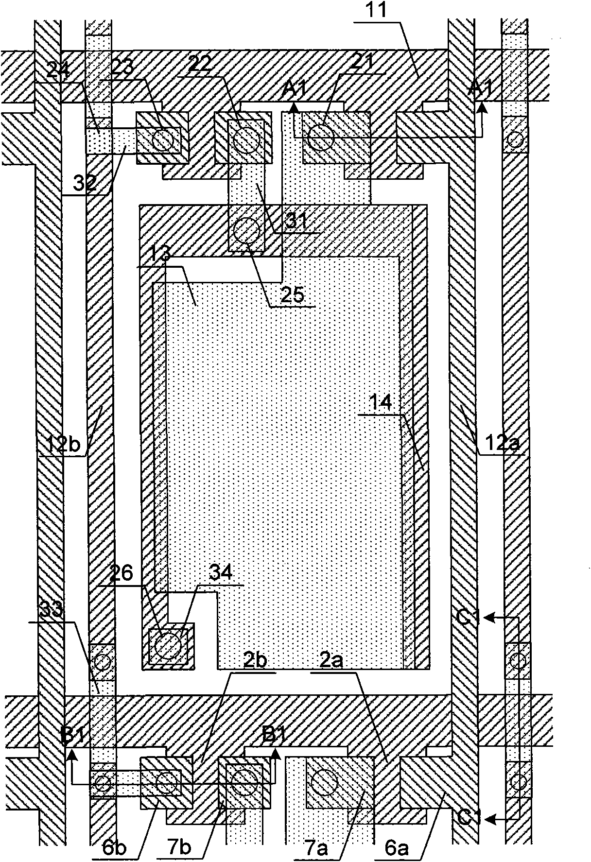
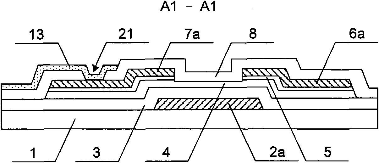
[0064] The technical solutions of the present invention will be described in further detail below with reference to the accompanying drawings and embodiments. The film thickness and area size and shape of each layer in the drawings do not reflect the true proportions of liquid crystal displays, TFT-LCD array substrates or color filter substrates, and the purpose is only to illustrate the content of the present invention.

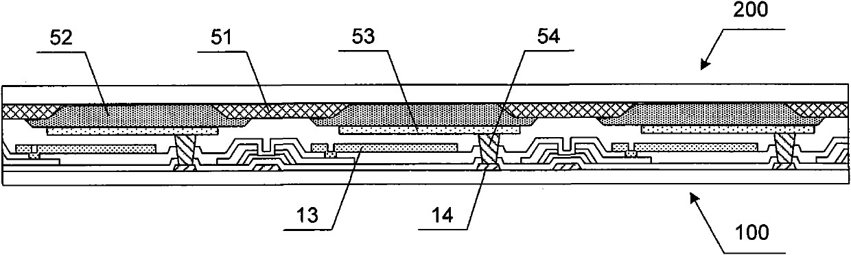
[0065] figure 1 It is a structural schematic diagram of the liquid crystal display of the present invention. Such as figure 1 As shown, the main structure of the liquid crystal display of the present invention includes a TFT-LCD array substrate 100 and a color filter substrate 200 that are boxed together with liquid crystal interposed therebetween. The gate line and the first data line are formed on the TFT-LCD array substrate 100 of the present invention, and the gate line and the first data line define several pixel areas arranged in a matrix, and each p...


PUM

PropertyMeasurementUnit
Diameteraaaaaaaaaa
Diameteraaaaaaaaaa

Abstract

The invention relates to a liquid crystal display and a manufacturing method thereof. The liquid crystal display comprises a thin film transistor liquid crystal display (TFT-LCD) array substrate and a color film substrate which are folded together and sandwich liquid crystal, wherein the TFT-LCD array substrate comprises a grid line, a first film transistor used for controlling a first data line to provide data voltage for a pixel electrode, and a second film transistor used for controlling a second data line to provide common voltage to a storage electrode line; and the color film substrate comprises mutually independent common electrodes electrically connected with the storage electrode line. The color film substrate is provided with the mutually independent common electrodes, and the film transistors controlling the common electrodes are arranged on the array substrate, so that the voltage difference between the pixel electrode and the common electrodes is kept unchanged; therefore, the display grayscale difference of pixels caused by different feedthrough effects of the pixels is eliminated and the display quality is improved.

Description

technical field [0001] The invention relates to a display and a method for manufacturing the display, in particular to a liquid crystal display and a method for manufacturing the same. Background technique [0002] The main structure of a Thin Film Transistor Liquid Crystal Display (TFT-LCD for short) includes an array substrate and a color filter substrate in a box-to-box arrangement. The array substrate is formed with gate lines, data lines, and thin film transistors arranged in a matrix. Pixel electrodes, black matrix, color resin and common electrodes are formed on the color filter substrate, the liquid crystal molecules are deflected by controlling the voltage difference between the pixel electrodes of the array substrate and the common electrodes of the color filter substrate, and the deflection angles of the liquid crystal molecules are different to make the transmission Different light sources produce different gray scales to achieve the display of the desired pictur...

Claims


Application Information

Patent Timeline
IPC IPC(8): G02F1/1362G02F1/1368H01L21/82
Inventor 赵鑫明星周伟峰张文余郭建
Owner BOE TECH GRP CO LTD
Features
  • R&D
  • Intellectual Property
  • Life Sciences
  • Materials
  • Tech Scout
  • Unparalleled Data Quality
  • Higher Quality Content
  • 60% Fewer Hallucinations
Learn More