Vacuum processing system and vacuum processing method of semiconductor processing substrate

A vacuum processing and vacuum processing chamber technology, applied in semiconductor/solid-state device manufacturing, electrical components, circuits, etc., can solve problems such as insufficient consideration and loss of wafer processing capacity, and achieve high productivity, suppression of cross-contamination, and low foreign matter. Effect

Inactive Publication Date: 2011-05-18
HITACHI HIGH-TECH CORP
View PDF2 Cites 5 Cited by
  • Summary
  • Abstract
  • Description
  • Claims
  • Application Information

AI Technical Summary

Problems solved by technology

[0009] In the prior art that does not sufficiently consider the productivity per unit installation area, the wafer processing capacity per unit installation area of ​​the devices constituting the vacuum processing system is lost.

Method used


Image

  • Vacuum processing system and vacuum processing method of semiconductor processing substrate
  • Vacuum processing system and vacuum processing method of semiconductor processing substrate
  • Vacuum processing system and vacuum processing method of semiconductor processing substrate

Examples


Embodiment Construction

[0046] Embodiments of a vacuum processing system and a vacuum processing method for a semiconductor substrate to be processed according to the present invention will be described in detail below with reference to the drawings.

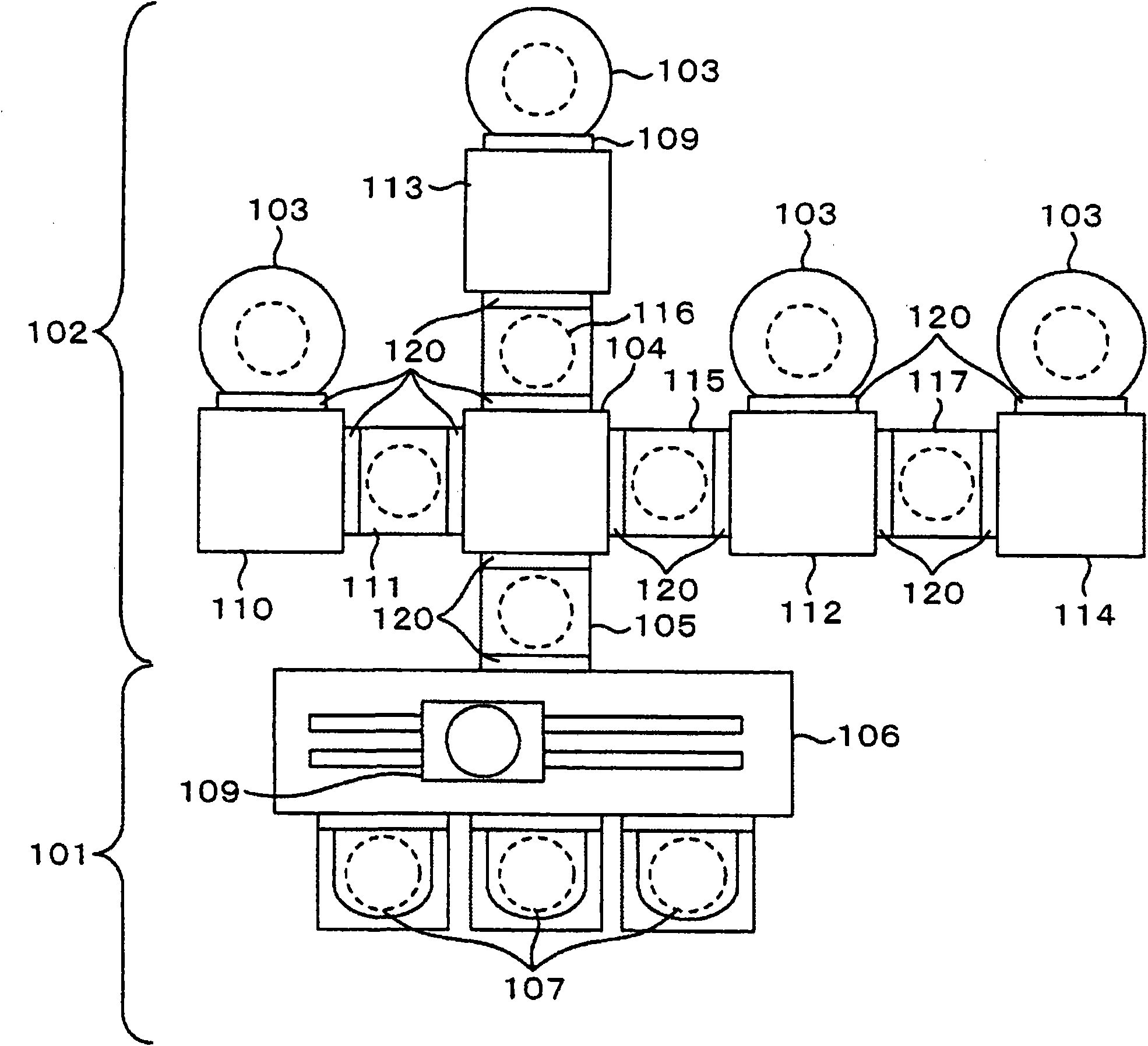
[0047] figure 1 The outline of the overall configuration of a vacuum processing system including a plurality of vacuum processing chambers 103 , 103 , 103 , 103 according to the first embodiment of the present invention will be described.

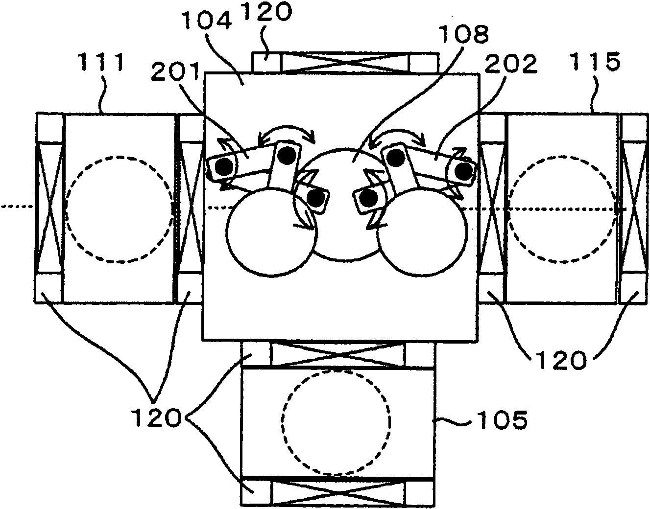
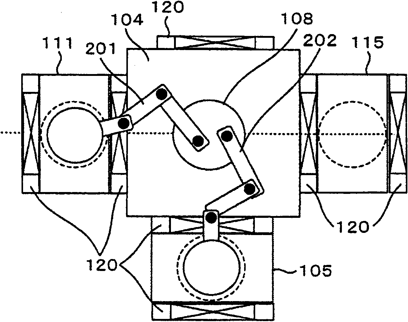
[0048] figure 1 The shown vacuum processing system 100 according to the first embodiment of the present invention including four vacuum processing chambers 103 , 103 , 103 , 103 is roughly divided into an atmosphere side module 101 and a vacuum side module 102 . The atmosphere side module 101 is a part that transports, accommodates, and locates the object to be processed, that is, semiconductor wafers, etc. under atmospheric pressure. processed modules. Furthermore, a lock chamber 105 is provided between the vacu...


PUM


Abstract

The invention provides a device, in which the arrangement of a vacuum processing chamber in a vacuum transfer chamber is optimized and the production performance of the objects to be processed in unit area is high. The invention provides a vacuum processing system of a semiconductor processing substrate and a vacuum processing method using the same, comprising an atmospheric transfer chamber having a plurality of cassette stands, a lock chamber arranged on a rear side of the atmospheric transfer chamber, and a first vacuum transfer chamber connected to a rear side of the lock chamber, wherein the first vacuum transfer chamber does not have any vacuum processing chamber connected thereto and has transfer intermediate chambers connected thereto, and the transfer intermediate chambers have subsequent vacuum transfer chambers connected thereto, and wherein the wafers are transferred via the lock chamber to the first vacuum transfer chamber to be processed in each of the subsequent vacuum processing chambers, which are further transferred via any of the transfer intermediate chambers connected to the first vacuum transfer chamber to the subsequent vacuum transfer chambers, and the respective wafers transferred to the subsequent vacuum transfer chambers other than the first vacuum transfer chamber are transferred to the respective vacuum processing chambers connected to each of the vacuum processing chambers and processed therein.

Description

technical field [0001] The present invention relates to a vacuum system provided with a transport mechanism for semiconductor substrates to be processed (hereinafter, including semiconductor wafers and substrate-shaped samples, etc., simply referred to as "wafers") between a vacuum processing chamber and a vacuum transfer chamber of a semiconductor processing apparatus. The composition of the processing system, and the vacuum processing method using the system. In particular, it relates to a configuration of a vacuum processing system and a vacuum processing method in which a plurality of vacuum processing chambers are arranged in series via a transfer mechanism in the plurality of vacuum transfer chambers. Background technique [0002] In such an apparatus, especially an apparatus that processes a processing object in a reduced-pressure apparatus, miniaturization and high precision of processing are sought, and improvement of processing efficiency of a processing object, th...

Claims


Application Information

Patent Timeline
Patent Type & Authority Applications(China)
IPC IPC(8): H01L21/67
CPCH01L21/67778H01L21/67184H01L21/67766H01L21/67196
Inventor 田内勤近藤英明仲田辉男野木庆太下田笃智田崇文
Owner HITACHI HIGH-TECH CORP
Why Eureka
Try Eureka