Surface emitting device

A surface light-emitting element and spectrum technology, applied in electrical components, laser components, lasers, etc., can solve the problems of inability to obtain mode gain and weakening of light confinement, and achieve the effect of increasing light output and increasing mode gain

Active Publication Date: 2013-03-13
MURATA MFG CO LTD
View PDF2 Cites 0 Cited by
  • Summary
  • Abstract
  • Description
  • Claims
  • Application Information

AI Technical Summary

Problems solved by technology

[0006] However, if the length of the resonator is extended and an active layer is further provided at a position corresponding to the antinode of the newly formed standing wave, since the optical length of the optical resonator becomes longer, the optical confinement becomes weaker, and there is a possibility that sufficient light cannot be obtained. The problem of modulus gain

Method used


Image

  • Surface emitting device
  • Surface emitting device
  • Surface emitting device

Examples


Embodiment Construction

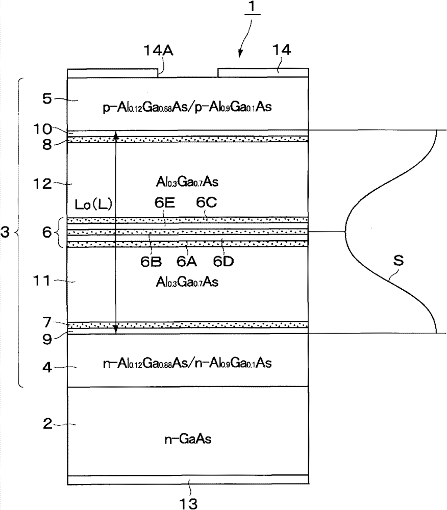
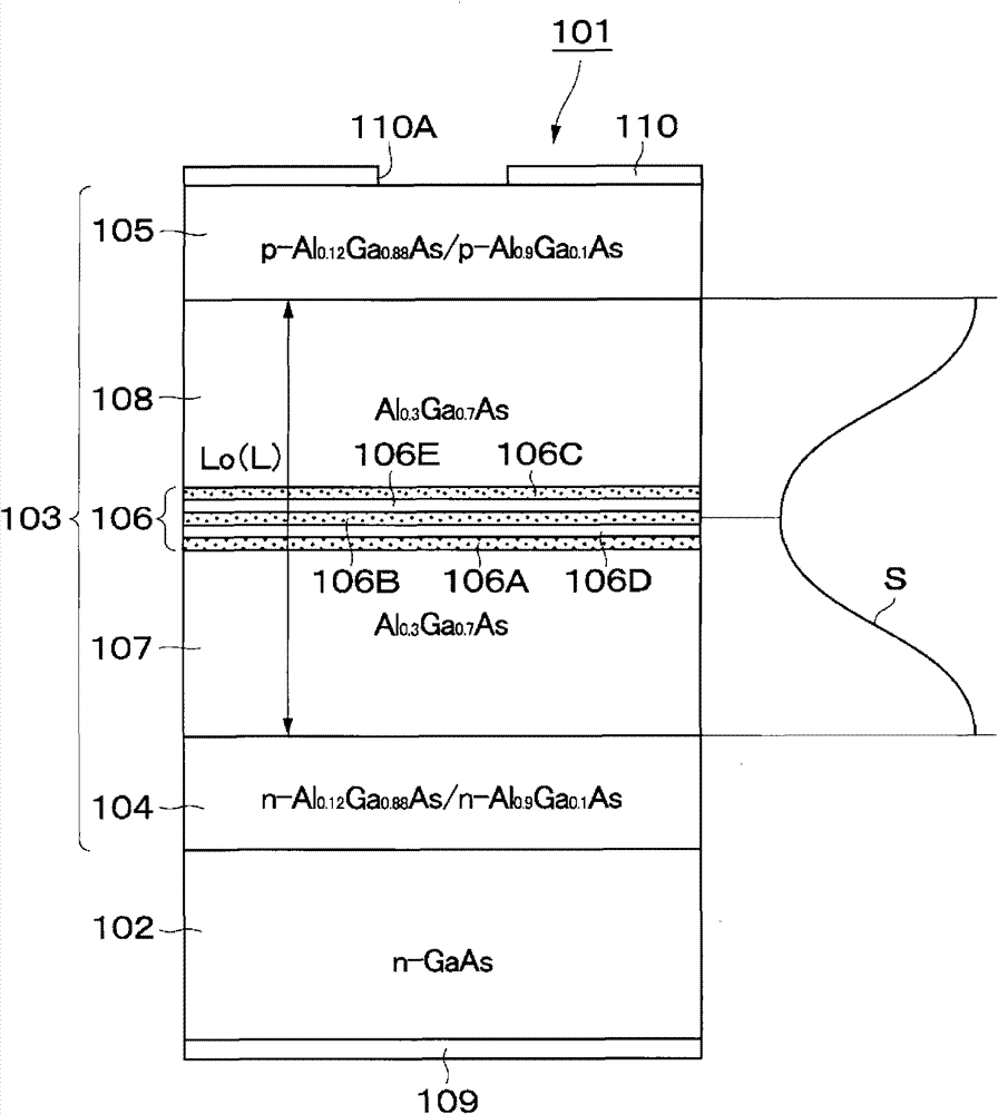
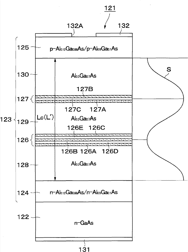
[0034] Hereinafter, as an embodiment of the present invention, a vertical cavity surface emitting laser element (hereinafter referred to as a VCSEL) will be described in detail with reference to the drawings.

[0035] First, use figure 1 , and the first embodiment will be described. The VCSEL 1 according to the first embodiment includes a lower reflective layer 4, a first barrier layer 9, a first sub active layer 7 (second active layer), a first cladding layer 11, and a main A stacked structure of active layer 6 (first active layer), second cladding layer 12 , second sub-active layer 8 (second active layer), second barrier layer 10 , and upper reflective layer 5 . The lower reflective layer 4, the first barrier layer 9, the first sub-active layer 7, the first cladding layer 11, the main active layer 6, the second cladding layer 12, the second sub-active layer 8, and the second barrier layer 10 and the upper reflective layer 5, forming an optical resonator 3. However, a curr...


PUM


Abstract

The invention relates to a surface emitting device for increasing a light limit coefficient so as to effectively increase a mode gain. A lower reflective layer (4) and an upper reflective layer (5) are respectively arranged at two end sides of a light resonator (3) in a thickness direction, and a primary active layer (6) is arranged at a central part of the light resonator (3) in the thickness direction; furthermore, aiming at the light resonator (3), a first secondary active layer (7) is arranged adjacent to the lower reflective layer (4), and a second secondary active layer (8) is arranged adjacent to the upper reflective layer (5); therefore, the first secondary active layer (7) and the secondary active layer (8) can be configured to a position of an antinode with large light amplitude without lengthening an optical length (Lo) between the lower reflective layer (4) and the upper reflective layer (5).

Description

technical field [0001] The present invention relates to surface emitting elements such as light emitting diodes (LEDs), vertical cavity surface emitting lasers (VCSELs) and the like. Background technique [0002] In general, the surface light-emitting element has a lower reflective layer of the first conductivity type, a plurality of barrier layers, and a single quantum well or multiple quantum wells formed between the barrier layers on the upper surface of the first conductivity type substrate. A stacked structure of a plurality of active layers and a second conductivity type upper reflective layer. Among them, a current narrowing layer for efficiently injecting current into the active layer is provided on either the lower reflective layer or the upper reflective layer. By forming such a configuration, an optical resonator is formed by the lower reflective layer, the plurality of barrier layers, the active layer, and the upper reflective layer. Among them, the pair of low...

Claims


Application Information

Patent Timeline
Patent Type & Authority Patents(China)
IPC IPC(8): H01S5/183H01S5/30
Inventor 楯敦次
Owner MURATA MFG CO LTD
Why Eureka
Try Eureka