Supercharge Your Innovation With Domain-Expert AI Agents!

Method for improving speed of seeking chips on probe table

A probe station and chip technology, which is applied in the photoengraving process of the pattern surface, the original for optical mechanical processing, optics, etc., to achieve the effect of improving the efficiency of testing and analysis

Inactive Publication Date: 2011-06-01
SHANGHAI HUA HONG NEC ELECTRONICS
View PDF0 Cites 0 Cited by
  • Summary
  • Abstract
  • Description
  • Claims
  • Application Information

AI Technical Summary

Problems solved by technology

[0003] In order to be able to quickly evaluate the failed chips, it is often necessary to be able to quickly identify each chip in the exposure unit on the probe station, especially when there are a large number of chips on a wafer, how can it be done on the probe station? Quickly find the chip you need to test, there is no better way

Method used


Image

  • Method for improving speed of seeking chips on probe table
  • Method for improving speed of seeking chips on probe table
  • Method for improving speed of seeking chips on probe table

Examples


Embodiment Construction

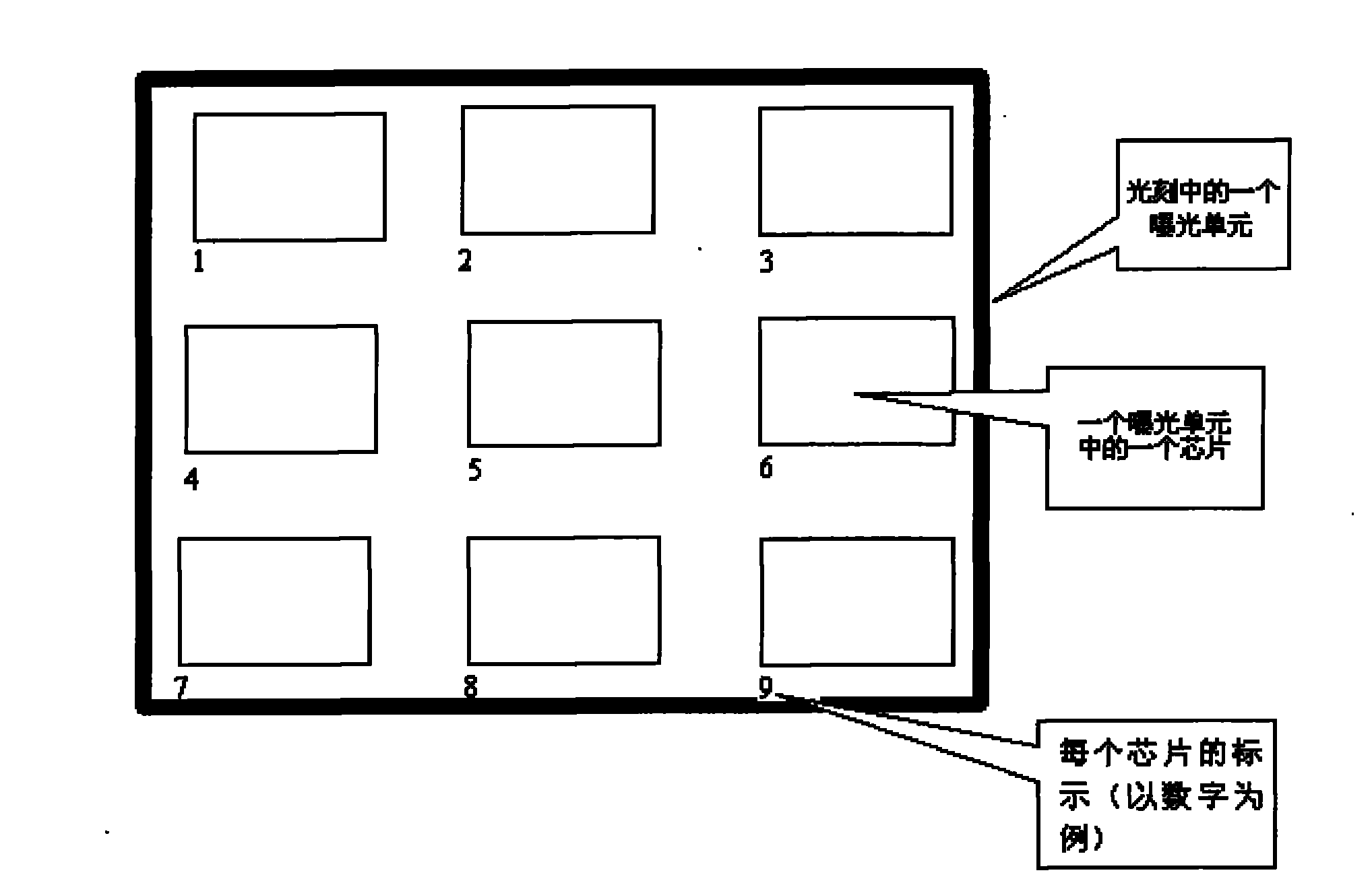
[0011] In order to achieve the purpose of rapid testing, the method for improving the speed of chip search on the probe station is to, when making the mask, on the top layer of metal of the mask, be located in the scribing groove around each chip Marks representing each chip are made at the same position to mark different chips. In this way, when there are many chips on a wafer, the chips to be tested can be quickly found on the probe station.

[0012] figure 1 For a lithography exposure unit and the relative positions of 9 chips in the exposure unit, marks for distinguishing different chips are marked on each chip.

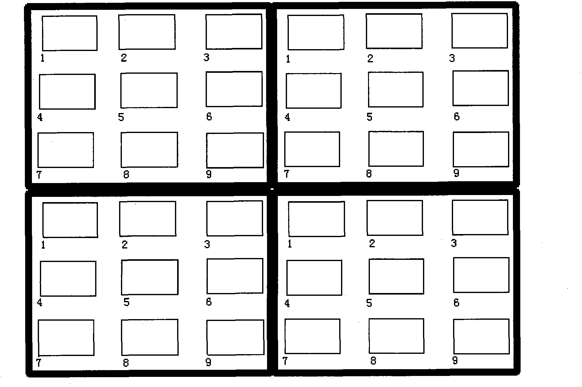
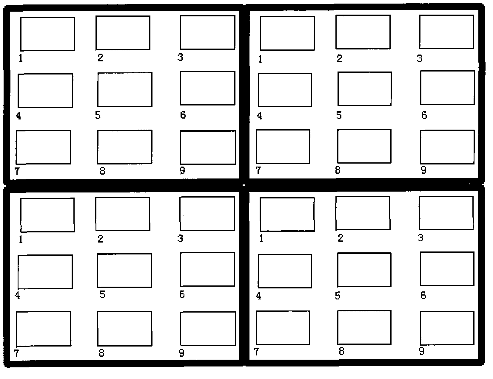
[0013] figure 2 It is a local position in a wafer composed of four photolithography exposure units, and it can be seen that each chip is marked with a specific mark.

[0014] The logo can be located at the upper left corner of each chip, or at other fixed positions relative to each chip.

[0015] The marks can use numbers, letters (such as English letters), ...


PUM


Abstract

The invention discloses a method for improving the speed of seeking chips on a probe table. When in manufacturing a maskplate, marks standing for various chip are manufactured on the top-layer metal of the maskplate positioned on the same position in a scribing sheet groove surrounding each chip, and are used for marking different chips; and when the number of the chips on each wafer is more, the chips needing to be tested can be rapidly sought on the probe table by the method provided by the invention, thus improving the efficiency of an analytic test.

Description

technical field [0001] The invention relates to the field of wafer-level testing of large-scale integrated circuits, in particular to a method capable of increasing chip search speed on a probe station. Background technique [0002] In the wafer-level testing process of existing large-scale integrated circuits, it is often found that the test results are related to the exposure unit (shot) during photolithography, and failures will occur at a fixed position in one exposure unit. [0003] In order to be able to quickly evaluate the failed chips, it is often necessary to be able to quickly identify each chip in the exposure unit on the probe station, especially when there are a large number of chips on a wafer, how can it be done on the probe station? There's no better way to quickly find the chips you need to test. Contents of the invention [0004] The technical problem to be solved by the present invention is to provide a method for improving the speed of chip search on ...

Claims


Application Information

Patent Timeline
Patent Type & Authority Applications(China)
IPC IPC(8): H01L21/00G03F1/00G03F1/38
Inventor 辛吉升桑浚之
Owner SHANGHAI HUA HONG NEC ELECTRONICS
Features
  • R&D
  • Intellectual Property
  • Life Sciences
  • Materials
  • Tech Scout
  • Unparalleled Data Quality
  • Higher Quality Content
  • 60% Fewer Hallucinations
Learn More