Three-dimensional semiconductor memory device

A storage device and semiconductor technology, applied in the fields of semiconductor devices, semiconductor/solid-state device manufacturing, and semiconductor/solid-state device components, etc., can solve problems such as reduced product reliability and reduced operating speed

Active Publication Date: 2011-06-29
SAMSUNG ELECTRONICS CO LTD
View PDF4 Cites 42 Cited by
  • Summary
  • Abstract
  • Description
  • Claims
  • Application Information

AI Technical Summary

Problems solved by technology

However, this new structure poses various problems, such as reduced reliability and / or reduced operating speed of the product

Method used


Image

  • Three-dimensional semiconductor memory device
  • Three-dimensional semiconductor memory device
  • Three-dimensional semiconductor memory device

Examples


no. 2 example

[0143] The same reference numerals are used to denote the same parts as those in the first embodiment of the inventive concept, and the description of the same parts will be omitted for the sake of brevity.

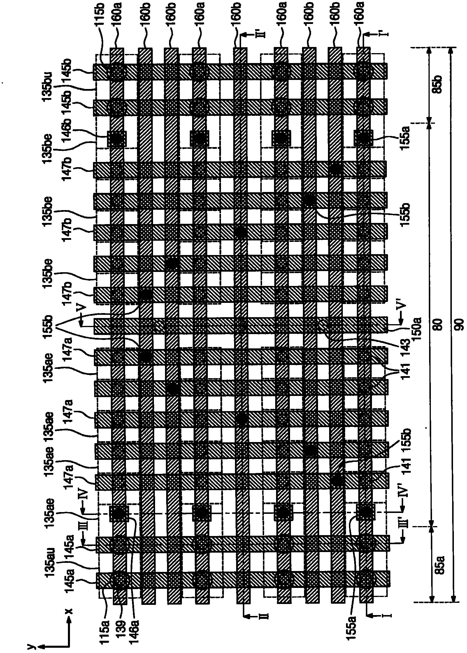
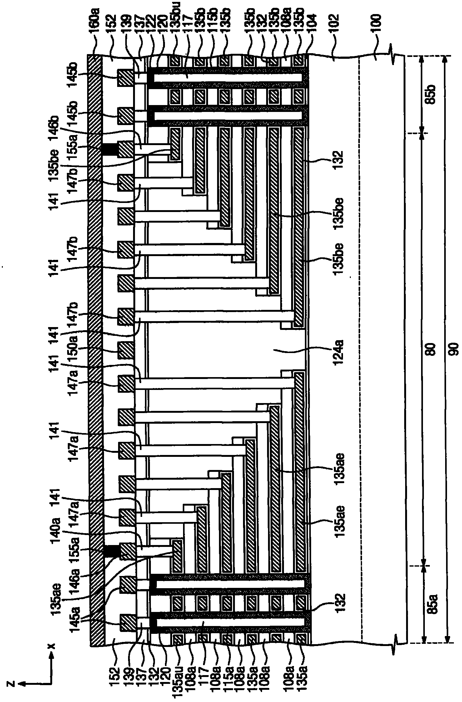
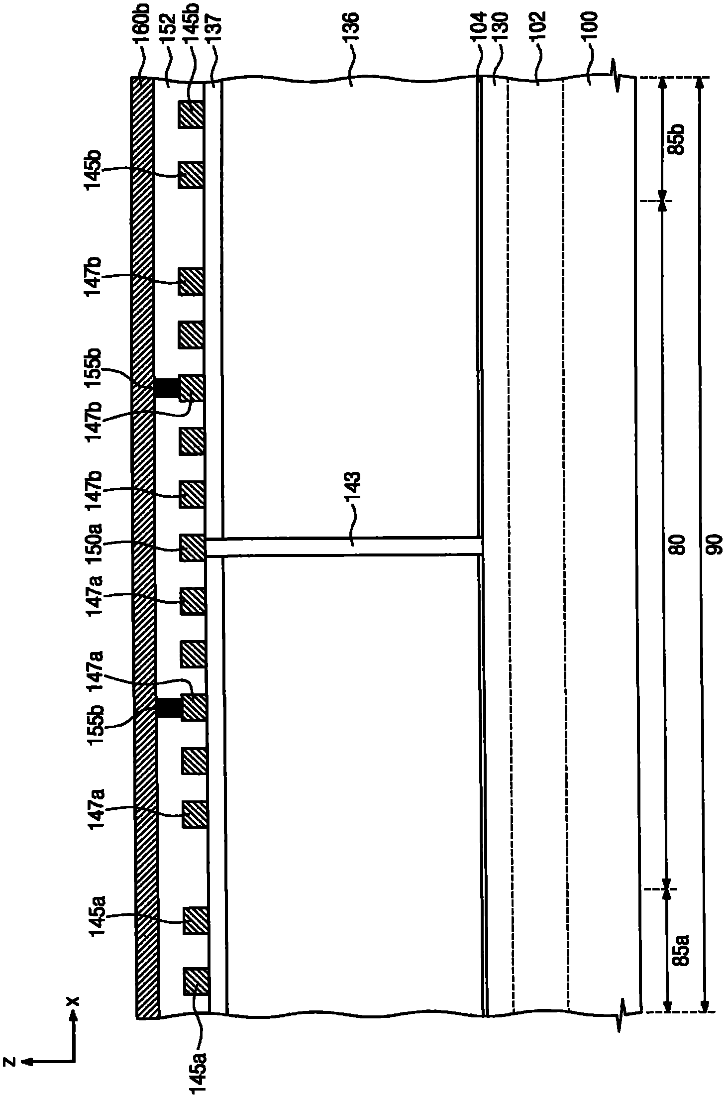
[0144] Picture 12 Is a perspective view showing a unit semiconductor memory device according to a second embodiment of the inventive concept. Figure 13 Yes Picture 12 A top view of the three-dimensional semiconductor storage device shown in. Figure 14 It is a top view showing a modified example of the three-dimensional semiconductor memory device according to the second embodiment of the inventive concept.

[0145] Reference Picture 12 with 13 , The three-dimensional semiconductor storage device may include a reference figure 1 , 2A -2E and image 3 The described vertical type string, conductive lines 150a, bit lines 145a and 145b, local interconnects 147a and 147b, and a second intermediate dielectric layer 152. A plurality of interconnections 260a and 260b may be provide...


PUM


Abstract

Provided is a three-dimensional semiconductor memory device. The three-dimensional semiconductor memory device includes a substrate that has a cell array region including a pair of sub-cell regions and a strapping region interposed between the pair of sub-cell regions. A Plurality of sub-gates are sequentially stacked on the substrate in each of the sub-cell regions, and interconnection components are electrically connected to extensions of the stacked sub-gates, respectively, which extend into the strapping region. Each of the interconnection components is electrically connected to the extensions of the sub-gate which are disposed in the pair of the sub-cell regions, respectively, and which are located at the same level.

Description

[0001] This application claims priority for Korean Patent Application No. 10-2009-0110975 filed with the Korean Intellectual Property Office on November 17, 2009, and the disclosure of this application is incorporated herein by reference. Technical field [0002] The present invention relates to semiconductor devices, and more particularly, to three-dimensional semiconductor storage devices. Background technique [0003] With the rapid development of the electronics industry, the requirements for the integration of semiconductor storage devices are constantly increasing. Integration is an important factor in determining product prices. For example, as the degree of integration increases, the price of semiconductor storage devices will decrease. For this reason, semiconductor devices especially require higher integration. Generally, since the integration degree of a semiconductor device can be determined by the two-dimensional area of ​​a unit memory cell, the integration degree ...

Claims


Application Information

Patent Timeline
Patent Type & Authority Applications(China)
IPC IPC(8): H01L27/105H01L23/528
CPCH01L27/11565H01L27/11578H01L21/02697H01L27/11582H01L21/02365H10B43/10H10B43/50H10B43/20H10B43/27H01L29/7841
Inventor 沈善一许星会金汉洙张在薰赵厚成
Owner SAMSUNG ELECTRONICS CO LTD
Why Eureka
Try Eureka