Manufacturing method of memory

A manufacturing method and memory technology, which are applied in semiconductor/solid-state device manufacturing, electrical components, circuits, etc., can solve the problems of difficulty, affect the size of the contact window, damage the first group of spacers, etc., and achieve good electrical insulation, good Effects of Component Properties

Active Publication Date: 2011-07-20
WINBOND ELECTRONICS CORP
View PDF4 Cites 8 Cited by
  • Summary
  • Abstract
  • Description
  • Claims
  • Application Information

AI Technical Summary

Problems solved by technology

[0004] However, since the openings between the gates of the memory cell region have a relatively large aspect ratio, it is not easy to remove the second group of spacer materials between the gates, and the removal process may first set of spacers
As a result, the first set of spacers cannot provide good electrical insulation for the gate, and affect the size of the subsequent contact window formed by using the first set of spacers

Method used


Image

  • Manufacturing method of memory
  • Manufacturing method of memory
  • Manufacturing method of memory

Examples


Embodiment Construction

[0026] In order to make the above-mentioned features and advantages of the present invention more comprehensible, the following specific embodiments are described in detail together with the accompanying drawings.

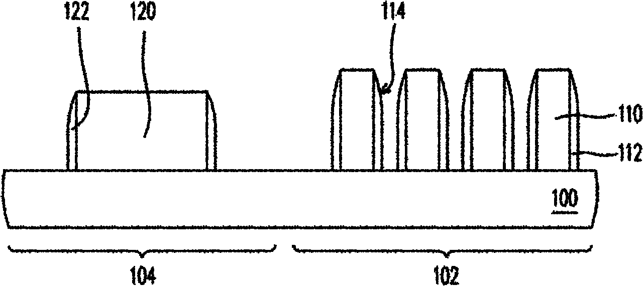
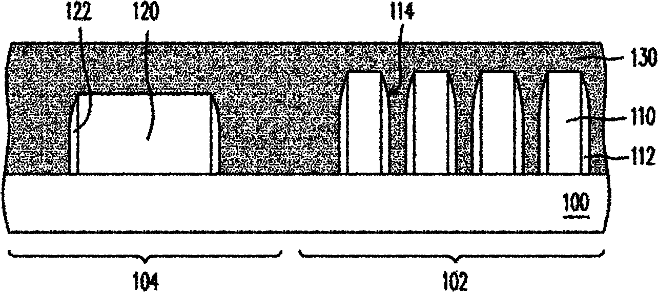
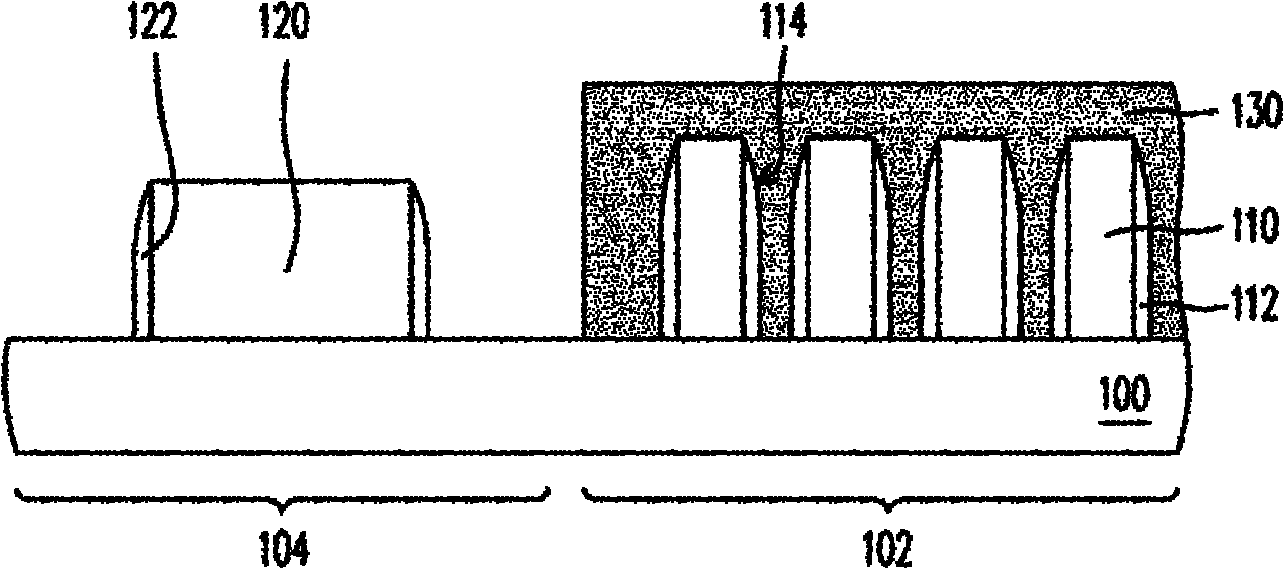
[0027] Figure 1A to Figure 1I is a schematic cross-sectional flow diagram of a manufacturing method of a memory according to an embodiment of the present invention, Figure 2A and Figure 2B respectively Figure 1A and Figure 1F The top view schematic diagram of the storage cell area, where Figure 1A and Figure 1F The storage cell area of Figure 2A and Figure 2B A schematic sectional view along line A-A', Figure 2A and Figure 2B The illustration of the spacer is omitted.

[0028] Please also refer to Figure 1A and Figure 2A , providing a substrate 100, the substrate 100 includes a memory cell region 102 and a peripheral region 104, a plurality of gates 110, 120 have been formed on the substrate 100, and first spacers 112, 122 are formed on the s...


PUM


Abstract

The invention provides a manufacturing method of a memory. The manufacturing method comprises the following steps of: providing a substrate comprising a memory cell region and a peripheral region, wherein a plurality of gates are formed on the substrate, the lateral wall of each gate is provided with a first clearance wall, and a plurality of openings are arranged among the gates of the memory cell region; forming a first material layer on the substrate of the memory cell region, wherein the first material layer covers the gates of the memory cell region and fills the openings; treating the peripheral region; removing a part of first material layer and forming first patterns in the openings; forming a second material layer on the substrate, wherein the second material layer covers the peripheral region and the memory cell region and exposes the first patterns; removing the first patterns and forming a plurality of contact window openings in the second material layer; and respectively forming a contact window plug in the contact window openings. In the invention, the clearance wall can provide favorable electric insulation for the gates, a self-aligned contact window is formed between the adjacent clearance walls, and therefore, the memory has favorable element characteristics.

Description

technical field [0001] The invention relates to a manufacturing method of a memory. Background technique [0002] Generally, as the size of the memory gradually shrinks, in order to overcome the increasingly smaller line width and prevent the misalignment of the contact, a self-aligned contact (SAC) process is adopted. [0003] In the self-aligned contact process, the thickness of the spacer on the sidewall of the gate will affect the size of the contact formed between the gates. However, since the memory device includes a memory cell region and a peripheral region, and the components in the memory cell region and the peripheral region have different requirements on the thickness of the spacer, the complexity of the process is increased. Generally speaking, the first group of spacers will be formed on the gate sidewalls of the memory cell region and the peripheral region at the same time, and then, in order to form the source and drain regions of the peripheral region, usua...

Claims


Application Information

Patent Timeline
Patent Type & Authority Applications(China)
IPC IPC(8): H01L21/8239H01L21/762
Inventor 蒋汝平廖修汉
Owner WINBOND ELECTRONICS CORP
Why Eureka
Try Eureka