Manufacturing method of photomask, photomask and manufacturing method of display device

A manufacturing method and photomask technology, which are applied in the direction of photolithography exposure device, microlithography exposure equipment, pattern surface photolithography technology, etc., can solve the problems of inability to read alignment marks, wrong recognition, the first main Insufficient coincidence accuracy of the pattern and the second pattern, etc.

Active Publication Date: 2011-08-03
HOYA CORP
View PDF4 Cites 7 Cited by
  • Summary
  • Abstract
  • Description
  • Claims
  • Application Information

AI Technical Summary

Problems solved by technology

As a result, there is no position where the alignment mark can be read in the second drawing process, and the alignment mark cannot

Method used


Image

  • Manufacturing method of photomask, photomask and manufacturing method of display device
  • Manufacturing method of photomask, photomask and manufacturing method of display device
  • Manufacturing method of photomask, photomask and manufacturing method of display device

Examples


no. 1 Embodiment approach

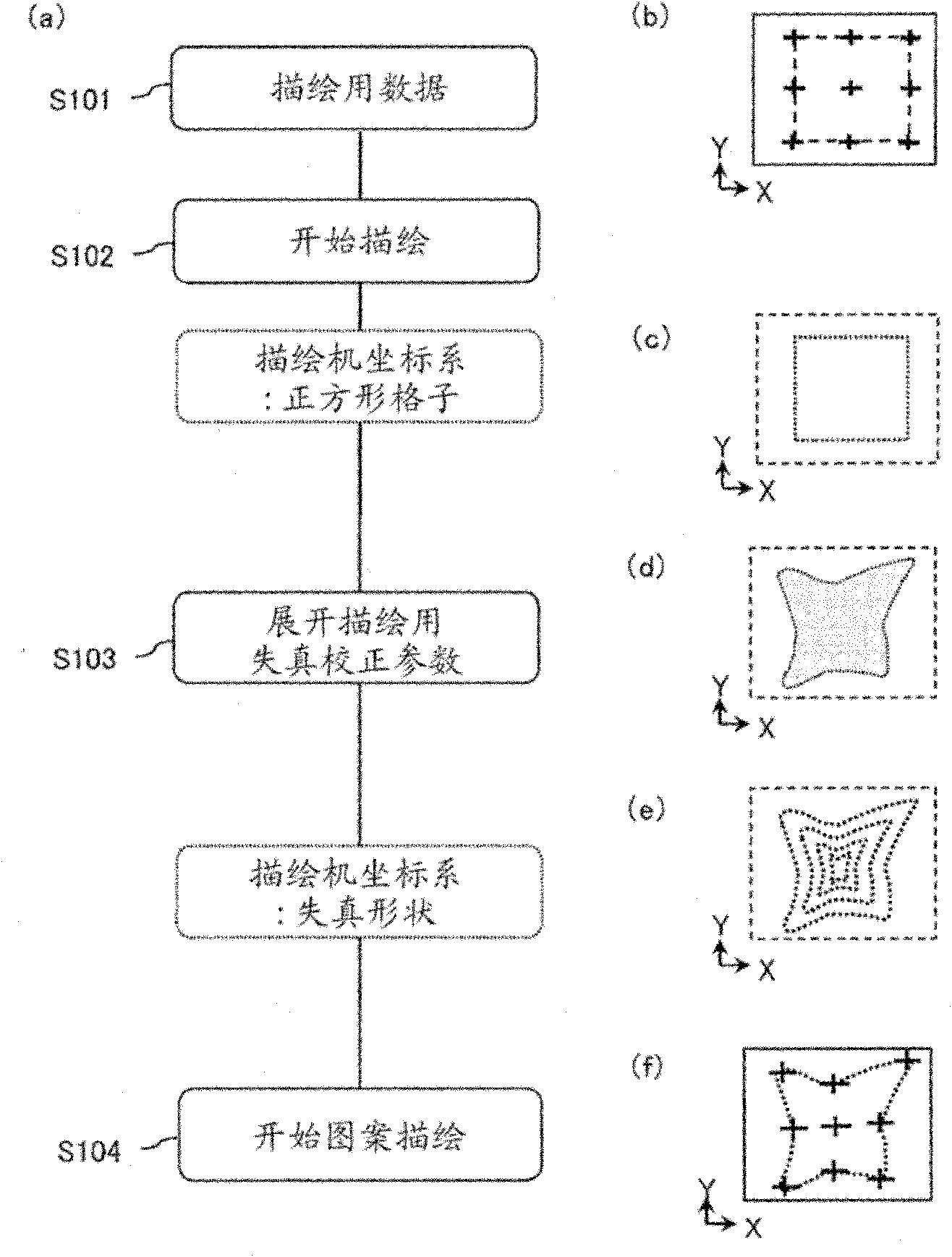
[0038] Below, the main reference Figure 7 , 3 4. The first embodiment of the present invention will be described. Figure 7 It is a flowchart of the manufacturing method of the multi-color photomask of this embodiment. image 3 It is a flowchart of the first drawing process of this embodiment, Figure 4 It is a flowchart of the second drawing process of this embodiment.

[0039] (1) Manufacturing method of multi-color photomask

[0040] First, refer to Figure 7 The outline of the manufacturing method of a multi-color photomask is demonstrated.

[0041] (Process of preparing mask blank)

[0042] A mask blank 100b is prepared in which a semi-transmissive film 111 as a second thin film and a light-shielding film 112 as a first thin film are sequentially formed on a transparent substrate 110 in advance ( Figure 7 (a)). In addition, a first resist film 133 made of, for example, a positive photoresist material is formed in advance on the light shielding film 112 .

[004...

no. 2 Embodiment approach

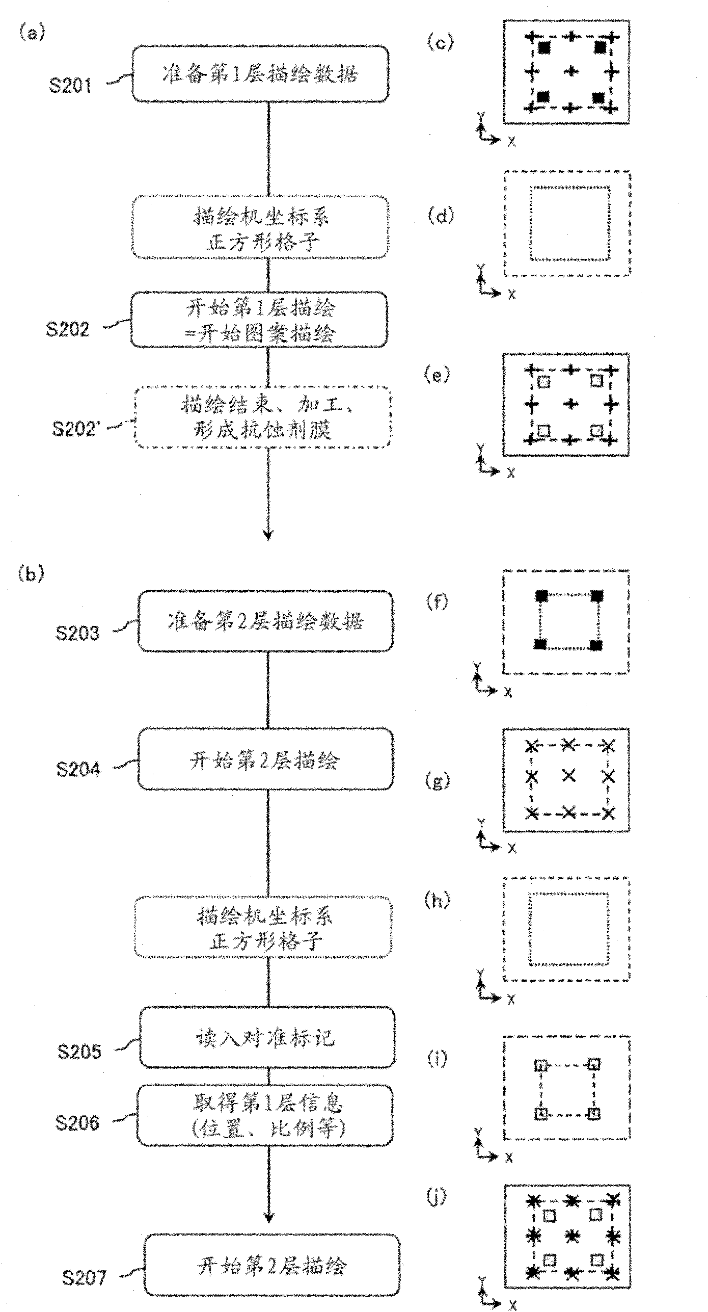
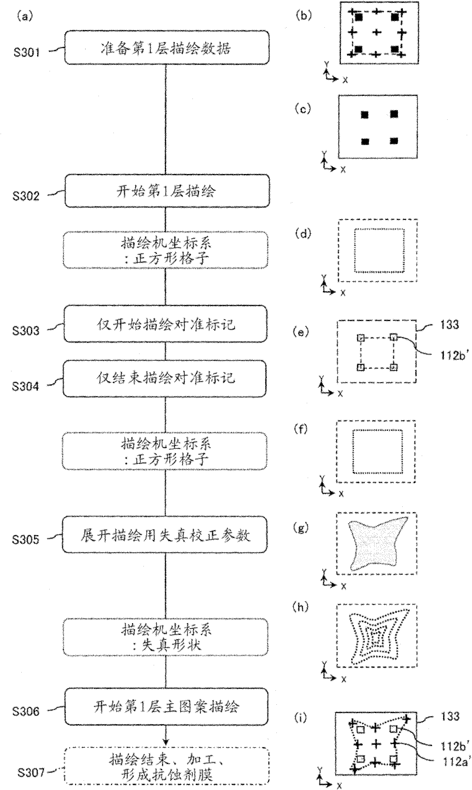
[0077]The first drawing step and the second drawing step of this embodiment are different from those of the first embodiment. Below, the main reference Figure 5 , 6 The drawing process of the present invention will be described. Figure 5 It is a flowchart of the first drawing process of this embodiment, Figure 6 It is a flowchart of the second drawing process of this embodiment.

[0078] (1st drawing process)

[0079] Such as Figure 5 As shown in (a), first, the first pattern data as the first layer drawing data is prepared (S501). Figure 5 (b) The structure of the 1st pattern data is illustrated. exist Figure 5 In (b), the alignment mark data is represented by - symbol, and the 1st main pattern data is represented by + symbol. In addition, in this embodiment, the drawing of the region 112 a ′ to be formed of the first main pattern and the drawing of the region 112 b ′ of an alignment mark to be formed are performed simultaneously. Therefore, the alignment mark ...


PUM


Abstract

The invention relates to a manufacturing method of a photomask, a photomask and a manufacturing method of a display device. The manufacturing method of a photomask comprises the following steps of: a first composition procedure for performing a photolithography process on a first film formed on a transparent substrate to form a first pattern, and a second composition procedure for performing a photolithography process on a second film formed on the transparent substrate to form a second pattern. The first composition procedure comprises a first depiction procedure, and the second composition procedure comprises a second depiction procedure; in the first depiction procedure and the second depiction procedure, depictions are performed using correction coordinate systems with the same distortion correction.

Description

technical field [0001] The present invention relates to a method of manufacturing a photomask, a photomask, and a method of manufacturing a display device. Background technique [0002] There is known a technique for correcting drawing data accompanying deformation of a substrate when a pattern is formed on a substrate or the like using an exposure machine. For example, when deformation occurs on a substrate to be exposed due to heat treatment or lamination, the drawing data may be corrected based on the deformation of the substrate (see Japanese Patent Application Laid-Open No. 9-15834). [0003] When manufacturing a display device such as an FPD (Flat Panel Display), an exposure step of transferring the pattern for transfer that the photomask has to a transfer target body using an exposure machine is performed. However, since the photomasks used in the manufacture of display devices such as FPDs are large, they tend to be warped when placed on an exposure machine, and the...

Claims


Application Information

Patent Timeline
IPC IPC(8): G03F1/14G03F1/08G03F1/00G03F7/20G03F1/36G03F1/76
CPCG03F1/70G03F7/2063G03F7/70308G03F9/7003H01L21/0274H01L21/0337
Inventor 樋渡忠夫田中敏幸
Owner HOYA CORP
Why Eureka
Try Eureka