Lead frame and chip packaging body
A technology of chip packaging and lead frame, which is applied in the direction of semiconductor devices, semiconductor/solid-state device parts, electric solid-state devices, etc., can solve the problems of cost increase and achieve the effect of cost reduction
- Summary
- Abstract
- Description
- Claims
- Application Information
AI Technical Summary
Problems solved by technology
Method used
Image

Examples
Embodiment Construction
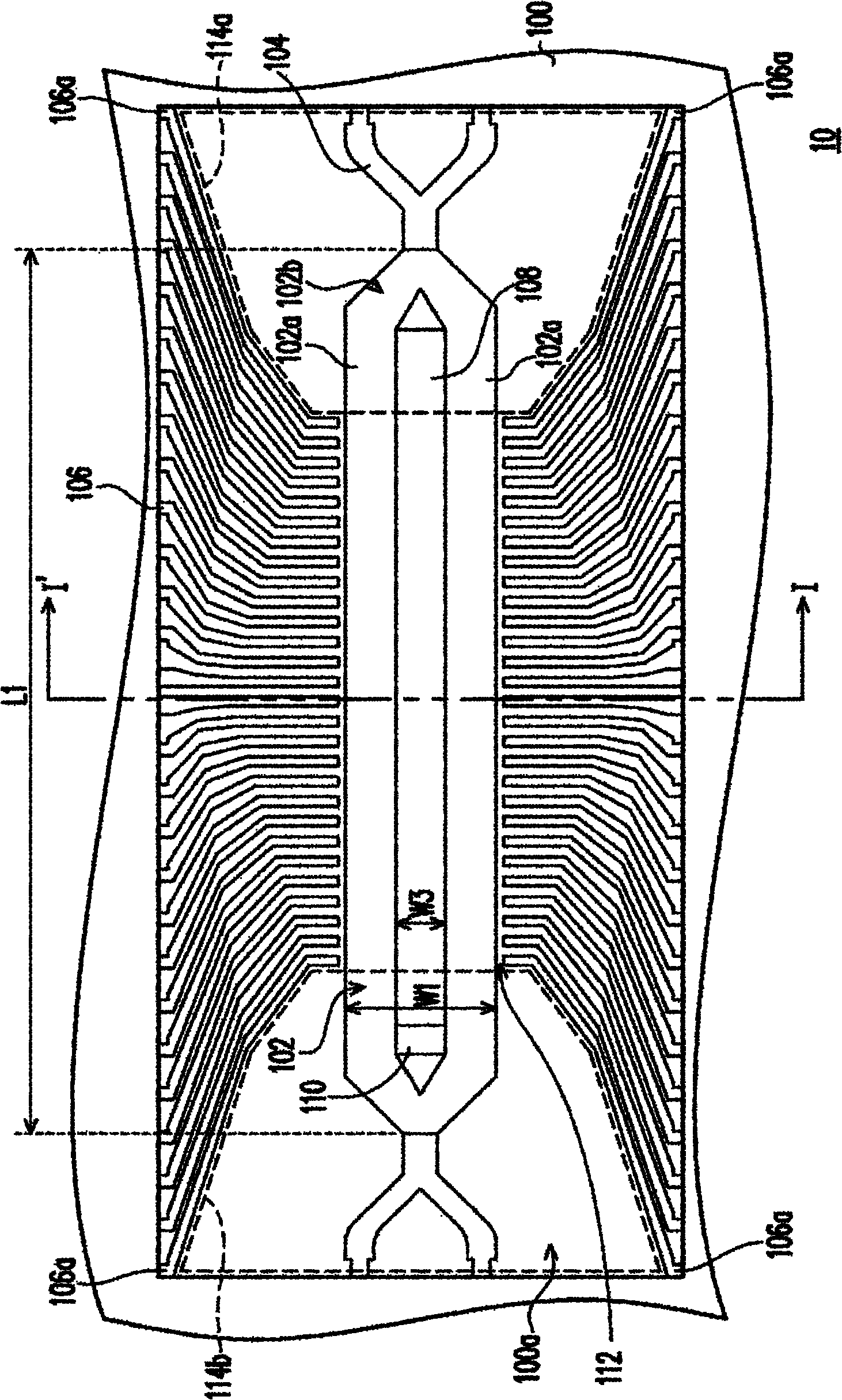
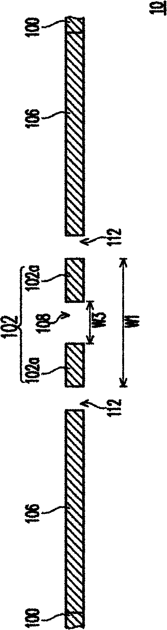
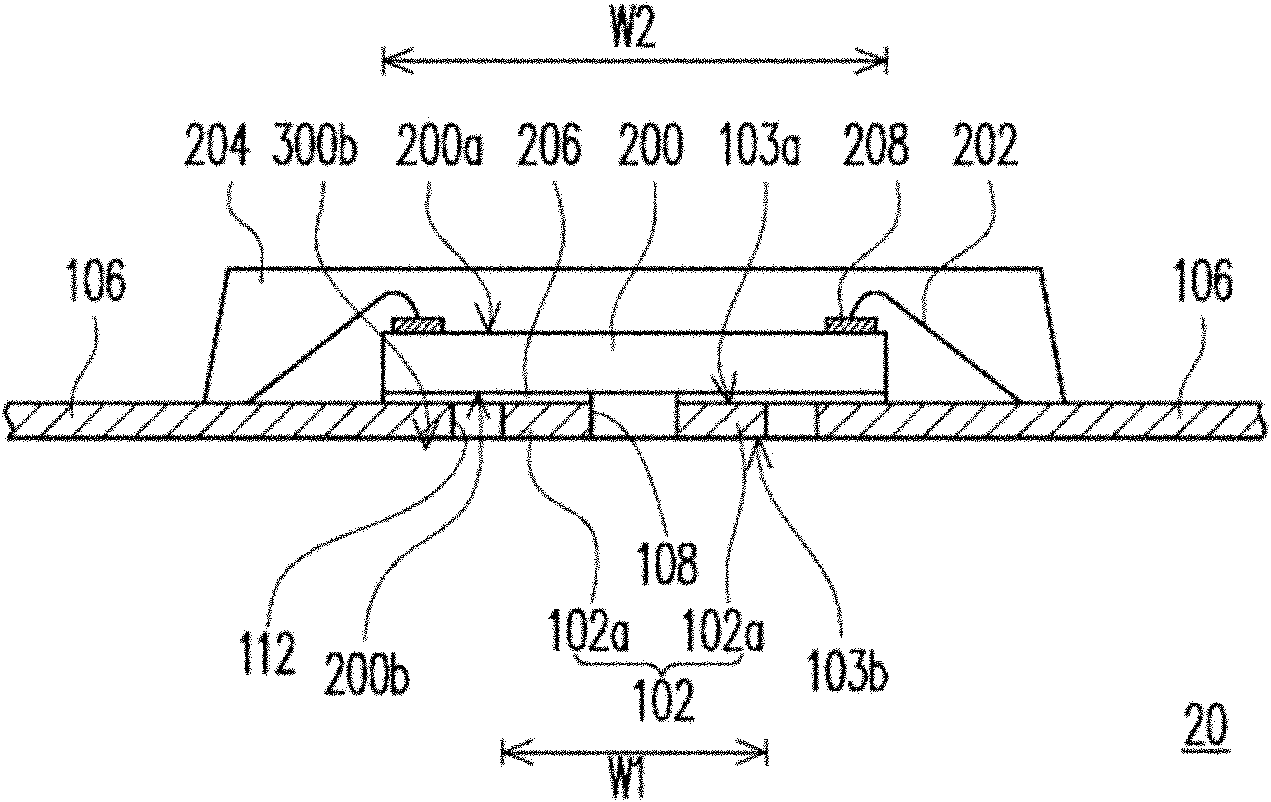
[0060] Figure 1A It is a schematic top view of a lead frame according to an embodiment of the present invention. Figure 1B for along Figure 1A The cross-sectional schematic diagram of the lead frame shown in the I-I' section in . Please also refer to Figure 1A and Figure 1B, the lead frame 10 includes a frame 100 , a die holder 102 , a connecting rod 104 and a pin 106 . The chip holder 102 is disposed in the package area 100 a surrounded by the frame 100 . In the present embodiment, the chip holder 102 includes two side-by-side carrying bars 102a. Both ends of the two carrying bars 102a are connected to form connecting portions 102b respectively. The connecting portion 102b can be in various shapes depending on actual needs, and is not limited to Figure 1A The shape shown in . The connecting rods 104 are connected between the frame 100 and the corresponding connecting portions 102 b to fix the relative position between the die holder 102 and the frame 100 . The conn...
PUM
 Abstract
Description
Claims
Application Information