Method for strengthening silicon-based thin film electroluminescence

A silicon-based thin film and luminescence technology, which is applied in circuits, electrical components, semiconductor devices, etc., can solve the problems of low electroluminescence efficiency of silicon-rich silicon nitride thin films, which are not enough for communication and data exchange, and achieve enhanced The effect of carrier injection efficiency, enhanced radiative recombination rate, and simple method

Inactive Publication Date: 2012-07-25
ZHEJIANG UNIV
View PDF0 Cites 0 Cited by
  • Summary
  • Abstract
  • Description
  • Claims
  • Application Information

AI Technical Summary

Problems solved by technology

However, the electroluminescence efficiency of silicon-rich silicon nitride thin films is still low, which is not enough to meet the requirements of silicon-based optoelectronics, which use light as the information carrier to propagate within a certain distance and realize data exchange.

Method used


Image

  • Method for strengthening silicon-based thin film electroluminescence
  • Method for strengthening silicon-based thin film electroluminescence
  • Method for strengthening silicon-based thin film electroluminescence

Examples


Embodiment 1

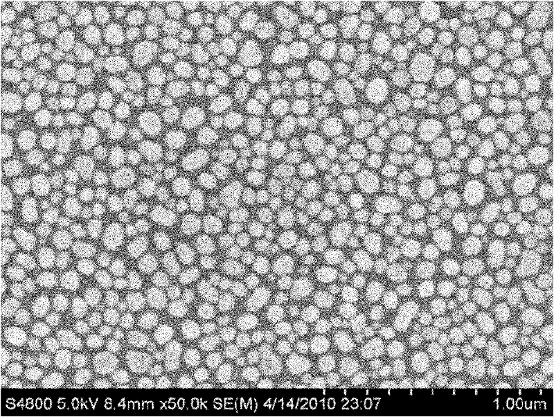
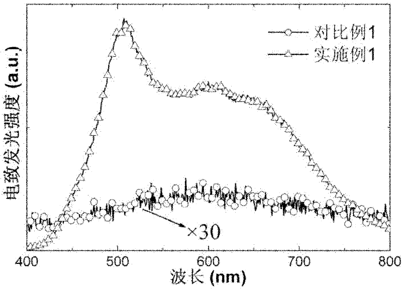
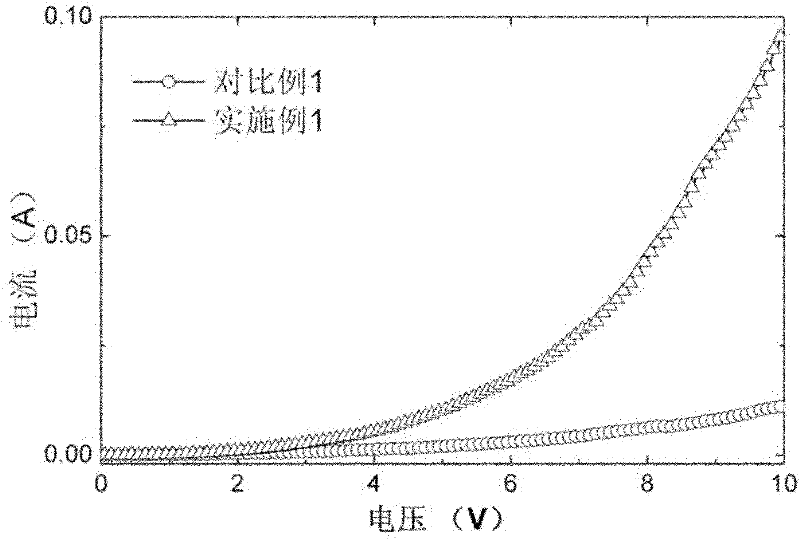
[0026] The P-type epitaxial silicon wafer (the substrate resistivity is less than 0.004Ω·cm, the epitaxial layer thickness is 11.4μm, and the resistivity is 2.5Ω·cm) is cleaned by standard RCA and the surface oxide layer is removed with hydrofluoric acid. The standard RCA cleaning steps are as follows: Put the P-type epitaxial silicon wafer into No. 1 cleaning solution (the volume ratio of ammonia water, hydrogen peroxide water and deionized water is 1:1:5), and put it in a water bath at about 80°C (80±5°C). Place it in the middle for 15 to 20 minutes; fully wash the P-type epitaxial silicon wafer with deionized water, put the cleaned P-type epitaxial silicon wafer into No. 2 cleaning solution (the volume ratio of hydrochloric acid, hydrogen peroxide and deionized water is 1:1: 6) Place it in a water bath at about 80°C (80±5°C) for 15-20 minutes, take it out and then wash it thoroughly with deionized water.

[0027] Then use electron beam evaporation (the size of the electron ...

Embodiment 2

[0037] The P-type epitaxial silicon wafer (the substrate resistivity is less than 0.004Ω·cm, the epitaxial layer thickness is 11.4μm, and the resistivity is 2.5Ω·cm) is cleaned by standard RCA and the surface oxide layer is removed with hydrofluoric acid. The standard RCA cleaning steps are as follows: Put the P-type epitaxial silicon wafer into No. 1 cleaning solution (the volume ratio of ammonia water, hydrogen peroxide water and deionized water is 1:1:5), and put it in a water bath at about 80°C (80±5°C). Place it in the middle for 15 to 20 minutes; fully wash the P-type epitaxial silicon wafer with deionized water, put the cleaned P-type epitaxial silicon wafer into No. 2 cleaning solution (the volume ratio of hydrochloric acid, hydrogen peroxide and deionized water is 1:1: 6) Place it in a water bath at about 80°C (80±5°C) for 15-20 minutes, take it out and then wash it thoroughly with deionized water.

[0038] Then use the method of DC magnetron sputtering (sputtering po...


PUM

PropertyMeasurementUnit
thicknessaaaaaaaaaa
electrical resistivityaaaaaaaaaa

Abstract

The invention discloses a method for strengthening silicon-based thin film electroluminescence, comprising the following steps: depositing a layer of silver thin film on the front of a P type silicon slice and carrying out thermal annealing so as to form a silver island thin film on the front of the P type silicon slice; depositing a layer of silicon-rich nitride thin film on the silver island thin film and depositing a layer of silicon oxide thin film on the layer of silicon-rich nitride thin film; and depositing a layer of indium tin oxide (ITO) thin film on the silicon oxide thin film as afront light-emitting electrode, and depositing a layer of aluminum on the back of the P type silicon slice as a back electrode so as to obtain a silicon substrate thin film luminescent device. The electroluminescence intensity of the silicon-based thin film luminescent device obtained by the method is obviously stronger than that of a common silicon thin film device; and the prepared silicon-based thin film luminescent device can work at higher output power and is not easy to puncture.

Description

technical field [0001] The invention belongs to the application field of silicon-based optoelectronics, and in particular relates to a method for enhancing the electroluminescence of silicon-based thin films. Background technique [0002] With the continuous reduction of the feature size of CMOS technology, the integration level of integrated circuits will become higher and higher, and the metal interconnection used for signal transmission between chips will become the bottleneck of device performance improvement. Silicon-based optoelectronics refers to the use of silicon-based materials to achieve light generation (convert electrical signals into optical signals), light propagation, light modulation, and light detection (convert optical signals into electrical signals), so as to realize information Propagation within a certain distance is one of the effective ways to solve the above-mentioned interconnection bottleneck. However, due to the indirect bandgap characteristics ...

Claims


Application Information

Patent Timeline
Patent Type & Authority Patents(China)
IPC IPC(8): H01L33/00
Inventor 李东升任常瑞王锋杨德仁
Owner ZHEJIANG UNIV
Why Eureka
Try Eureka