Silicon-based LED and preparation method thereof

A silicon-based and silicon-substrate technology, applied in electrical components, nanotechnology, circuits, etc., can solve problems such as low luminous efficiency, and achieve the effects of increasing light output, increasing electroluminescent intensity, and increasing brightness

Inactive Publication Date: 2021-06-25
GUIZHOU MINZU UNIV
View PDF1 Cites 0 Cited by
  • Summary
  • Abstract
  • Description
  • Claims
  • Application Information

AI Technical Summary

Problems solved by technology

[0003] As we all know, silicon is an abundant semiconductor material in the earth's crust, and silicon is non-toxic and harmless, but bulk silicon is an indirect band gap semiconductor, and the recombination of electrons and holes requires the assistance of phonons, so its luminous efficiency is extremely low

Method used


Image

  • Silicon-based LED and preparation method thereof
  • Silicon-based LED and preparation method thereof
  • Silicon-based LED and preparation method thereof

Examples


Embodiment 1

[0047] A method for preparing a silicon-based LED, comprising the following steps:

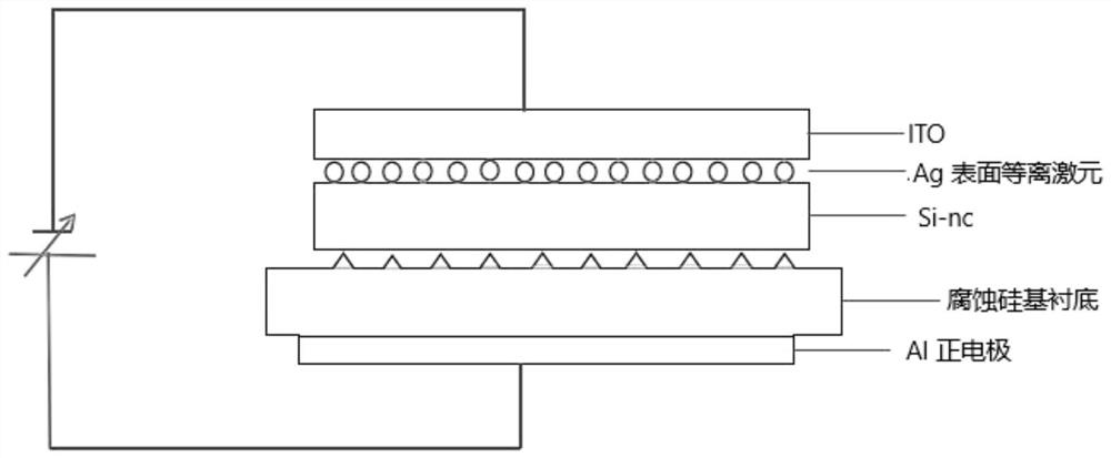
[0048] S1. Silver film evaporation: put Ag with a purity of 99.99% into a molybdenum boat, and place it in a vacuum of 4×10 -4 Evaporation is carried out in a Pa environment. In order to ensure the compactness of the evaporated silver film, the evaporation rate is: 0.04nm / s, and the thickness is 10nm. The silver film is evaporated on the p-type silicon substrate.

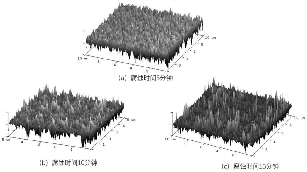
[0049] S2. Preparation of a rough silicon-based substrate: place the side of the silicon substrate with the silver film attached in H 2 O:H 2 o 2 : HF=8:4:1 mixed solution for etching, the etching time is 5 minutes, to obtain a silicon-based substrate with a rough surface, such as figure 2 shown.

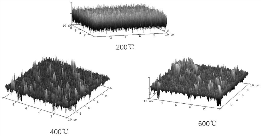
[0050] S3. Silicon nanocrystalline film: SiO and SiO with a purity of 99.99% 2 Put them into the molybdenum boat and molybdenum crucible respectively, and the vacuum degree is 4×10 -4 Under the Pa environment, thermal evaporation a...

Embodiment 2

[0057] S1. Silver film evaporation: put Ag with a purity of 99.99% into a molybdenum boat, and place it in a vacuum of 4×10 -4 Evaporation is carried out in a Pa environment. In order to ensure the compactness of the evaporated silver film, the evaporation rate is: 0.04nm / s, and the thickness is 10nm. The silver film is evaporated on the p-type silicon substrate.

[0058] S2. Preparation of a rough silicon-based substrate: place the side of the silicon substrate with the silver film attached in H 2 O:H 2 o 2 : HF=8:4:1 mixed solution for etching, and the etching time is 10 minutes to obtain a silicon-based substrate with a rough surface, such as figure 2 shown.

[0059] S3. Silicon nanocrystalline film: SiO and SiO with a purity of 99.99% 2 Put them into the molybdenum boat and molybdenum crucible respectively, and the vacuum degree is 4×10 -4 Under the Pa environment, thermal evaporation and electron beam heating are used for evaporation, and the evaporation rate is: 0....

Embodiment 3

[0066] S1. Silver film evaporation: put Ag with a purity of 99.99% into a molybdenum boat, and place it in a vacuum of 4×10 -4 Evaporation is carried out in a Pa environment. In order to ensure the compactness of the evaporated silver film, the evaporation rate is: 0.04nm / s, and the thickness is 10nm. The silver film is evaporated on the p-type silicon substrate.

[0067] S2. Preparation of a rough silicon-based substrate: place the side of the silicon substrate with the silver film attached in H 2 O:H 2 o 2 : HF=8:4:1 mixed solution for etching, the etching time is 15 minutes, to obtain a silicon-based substrate with a rough surface, such as figure 2 shown.

[0068] S3. Silicon nanocrystalline film: SiO and SiO with a purity of 99.99% 2 Put them into the molybdenum boat and molybdenum crucible respectively, and the vacuum degree is 4×10 -4 Under the Pa environment, thermal evaporation and electron beam heating are used for evaporation, and the evaporation rate is: 0.08n...


PUM

PropertyMeasurementUnit
thicknessaaaaaaaaaa
thicknessaaaaaaaaaa
thicknessaaaaaaaaaa

Abstract

The invention relates to a preparation method of a silicon-based LED, which comprises the steps of arranging a layer of silver film on the polished side surface of a silicon substrate, and corroding the silicon substrate to obtain a silicon-based substrate with a rough surface; arranging a layer of silicon nanocrystalline film on the surface of the silicon-based substrate; arranging a layer of surface plasmon on the side, which is away from the silicon-based substrate, of the silicon nanocrystalline film; arranging a negative electrode region on the side, which is away from the silicon nanocrystalline film, of the surface plasmon; and arranging a positive electrode region on the side, which is away from the silver film, of the silicon-based substrate. The brightness of the silicon-based LED can be effectively improved by adopting a two-step method, firstly, a silicon-based substrate with a rough surface is prepared by adopting a corrosion method, secondly, the luminous intensity of the silicon-based LED is improved through surface plasmons, the surface plasmons generate a surface plasma field under external bias voltage, and the surface plasma field increases the recombination probability of electrons and holes, so that the electroluminescence intensity of the silicon-based LED can be improved.

Description

technical field [0001] The invention belongs to the technical field of semiconductors, and in particular relates to a silicon-based LED and a preparation method thereof. Background technique [0002] Since the 21st century, silicon-based optoelectronic integration is considered to be the most promising way to solve chip-to-chip transmission in integrated circuits, and has gradually stepped out of the laboratory and into the process of industrialization. Despite such encouraging progress, there is still a bottleneck restricting the development of silicon-based optoelectronics—the lack of silicon lasers or silicon light-emitting diodes with high conversion efficiency. [0003] As we all know, silicon is an abundant semiconductor material in the earth's crust, and silicon is non-toxic and harmless, but bulk silicon is an indirect band gap semiconductor, and the recombination of electrons and holes requires the assistance of phonons, so its luminous efficiency is extremely low. ...

Claims


Application Information

Patent Timeline
Patent Type & Authority Applications(China)
IPC IPC(8): H01L33/22H01L33/02H01L33/36H01L33/00B82Y30/00
CPCH01L33/22H01L33/02H01L33/36H01L33/0054B82Y30/00
Inventor 陈家荣彭麦菊龙标吴凯生
Owner GUIZHOU MINZU UNIV
Why Eureka
Try Eureka