Preparation method of high-performance aluminum-doped cadmium sulfide silicon-based heterojunction light-emitting diode

A light-emitting diode and cadmium sulfide technology, which is applied in semiconductor devices, electrical components, circuits, etc., can solve the problems of low energy consumption, high energy consumption, and low luminous efficiency of diodes, so as to increase carrier mobility and reduce The effect of starting the operating voltage and improving the luminous efficiency

Inactive Publication Date: 2020-12-01
HENAN POLYTECHNIC UNIV
View PDF4 Cites 0 Cited by
  • Summary
  • Abstract
  • Description
  • Claims
  • Application Information

AI Technical Summary

Problems solved by technology

[0004] Aiming at the deficiencies of the prior art, the present invention provides a high-performance preparation method of aluminum-doped cadmium sulfide silicon-based heterojunction light-emitting diodes, which has the advantages of low energy consumption and high luminous efficiency, and solves the problem of high energy consumption of previous diodes. and the problem of low luminous efficiency

Method used


Image

  • Preparation method of high-performance aluminum-doped cadmium sulfide silicon-based heterojunction light-emitting diode
  • Preparation method of high-performance aluminum-doped cadmium sulfide silicon-based heterojunction light-emitting diode
  • Preparation method of high-performance aluminum-doped cadmium sulfide silicon-based heterojunction light-emitting diode

Examples


preparation example Construction

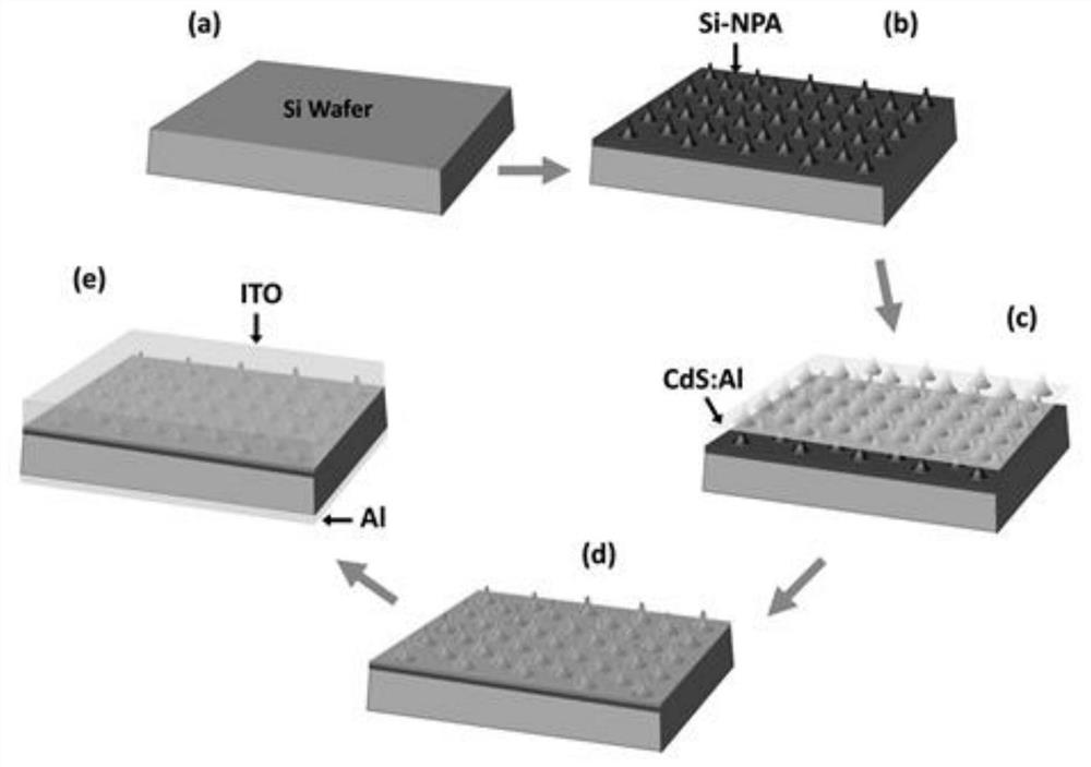
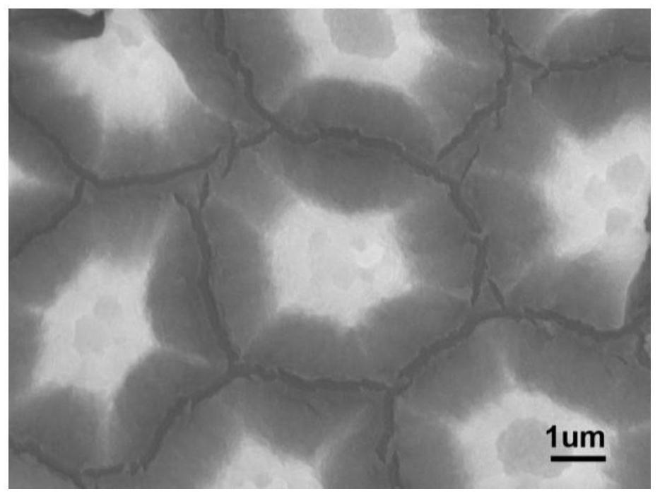
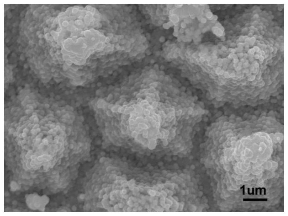
[0039] (1) Preparation and post-processing of P-type nanoporous silicon columnar arrays

[0040] The process of preparing P-type nanoporous silicon columnar arrays by hydrothermal etching method is as follows: (1) Firstly, soak the cut P-type heavily doped single crystal silicon wafer in acetone or ethanol solution for 5 minutes to remove surface organic pollutants , and then deep clean it using the standard RCA cleaning process. (2) Fix the cleaned silicon wafer on the sample holder, put it vertically into the hydrothermal reaction kettle, inject the prepared corrosion solution (0.03mol / L ferric nitrate nonahydrate, 13mol / L hydrofluoric acid) into the reaction kettle Acid and deionized water composition, reactor filling degree 83%). (3) Put the reactor into a drying oven, raise the temperature to 142°C, keep it warm for 45 minutes, take it out from the drying oven, cool for 60 minutes and open the cover, then cool to room temperature and take out the corroded silicon wafer f...

Embodiment 1

[0048] A method for preparing a high-performance aluminum-doped cadmium sulfide silicon-based heterojunction light-emitting diode, comprising the following steps:

[0049] Step A. Soak the cut P-type heavily doped monocrystalline silicon wafer in acetone or ethanol solution to remove surface organic pollutants, and then perform deep cleaning with standard RCA cleaning process;

[0050] Step B. Fix the cleaned silicon wafer on the sample holder, put it vertically into the hydrothermal reaction kettle, and inject the prepared etching solution into the reaction kettle;

[0051] Step C, putting the reaction kettle into a drying oven, first heating up, and then heat preservation;

[0052] Step D, take it out from the drying oven, cool for 60 minutes and open the cover, then cool to room temperature, take out the corroded silicon wafer from the reaction kettle, rinse it repeatedly with deionized water, and dry it naturally to obtain the nanoporous silicon columnar array;

[0053] S...

Embodiment 2

[0061] A method for preparing a high-performance aluminum-doped cadmium sulfide silicon-based heterojunction light-emitting diode, comprising the following steps:

[0062] Step A. Soak the cut P-type heavily doped monocrystalline silicon wafer in acetone or ethanol solution to remove surface organic pollutants, and then perform deep cleaning with standard RCA cleaning process;

[0063] Step B. Fix the cleaned silicon wafer on the sample holder, put it vertically into the hydrothermal reaction kettle, and inject the prepared etching solution into the reaction kettle;

[0064] Step C, putting the reaction kettle into a drying oven, first heating up, and then heat preservation;

[0065] Step D, take it out from the drying oven, cool for 60 minutes and open the cover, then cool to room temperature, take out the corroded silicon wafer from the reaction kettle, rinse it repeatedly with deionized water, and dry it naturally to obtain the nanoporous silicon columnar array;

[0066] S...


PUM


Abstract

The invention relates to the technical field of semiconductor light-emitting devices, and discloses a fabrication method of a high-performance aluminum-doped cadmium sulfide silicon-based heterojunction light-emitting diode. The fabrication method comprises the following steps of firstly, sequentially performing initial washing and deep washing on a P-type heavily-doping single-crystal silicon wafer with acetone or ethyl alcohol and standard RCA cleaning flow; secondly, fabricating a nanometer porous silicon columnar array by a hydrothermal corrosion method; and finally, taking the nanometer porous silicon columnar array as a substrate and aluminum nitride as a doping agent, and fabricating an aluminum-doped cadmium sulfide nanometer thin film and the nanometer porous silicon columnar array by a chemical water bath method. The aluminum-doped cadmium sulfide nanometer thin film and the nanometer porous silicon columnar array are organically combined and built to a novel light-emitting diode, and the array and porous structure of the nanometer porous silicon columnar array can be fully utilized; and meanwhile, by relatively high carrier mobility of the cadmium sulfide and the nanometer porous silicon columnar array after doping, the carrier recombination efficiency can be effectively improved, and the light-emitting efficiency of the light-emitting diode is improved.

Description

technical field [0001] The invention relates to the technical field of semiconductor light-emitting devices, in particular to a method for preparing a high-performance aluminum-doped cadmium sulfide silicon-based heterojunction light-emitting diode. Background technique [0002] Cadmium sulfide is a wide-bandgap compound semiconductor with a direct bandgap. It has the characteristics of high thermal conductivity, high electron mobility and good chemical stability. It is recognized as an ideal luminescent material and is widely used in the manufacture of yellow-green luminescence. diode. Silicon is the core material of contemporary electronic devices, which has the advantages of mature preparation technology and easy device integration. However, due to the differences in lattice constant, lattice structure, and thermal expansion coefficient between CdS and Si, it is difficult to directly grow CdS on Si substrates due to serious lattice mismatch, internal stress, etc. , and ...

Claims


Application Information

Patent Timeline
Patent Type & Authority Patents(China)
IPC IPC(8): H01L33/00H01L33/22H01L33/28H01L33/34
CPCH01L33/005H01L33/22H01L33/285H01L33/346
Inventor 闫玲玲蔡红新陈亮王永强杨鹏刘媛媛
Owner HENAN POLYTECHNIC UNIV
Why Eureka
Try Eureka