
Printed circuit board copper-coating method and copper-coated printed circuit board

A printed circuit board and printed circuit technology, which is applied to printed circuit parts, printed circuit assembly of electrical components, and electrical connection of printed components, etc. It can solve uneven soldering surface, falling off, virtual soldering and broken solder joints of PCB, etc. problems, to achieve the effect of reducing the degree of deformation, reducing the rate of defective welding and assembly, and reducing manufacturing costs

Inactive Publication Date: 2014-06-25
SHENZHEN SKYWORTH DIGITAL TECH CO LTD
View PDF6 Cites 0 Cited by
  • Summary
  • Abstract
  • Description
  • Claims
  • Application Information

AI Technical Summary

Problems solved by technology

It can solve the problem that the soldering surface of the PCB is uneven due to the difference in thermal expansion coefficient between the PCB insulation material and the copper skin during the reflow soldering process, resulting in virtual soldering and disconnection or even solder joints falling off.

Method used


Image

  • Printed circuit board copper-coating method and copper-coated printed circuit board
  • Printed circuit board copper-coating method and copper-coated printed circuit board
  • Printed circuit board copper-coating method and copper-coated printed circuit board

Examples


Embodiment Construction

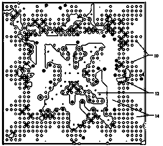
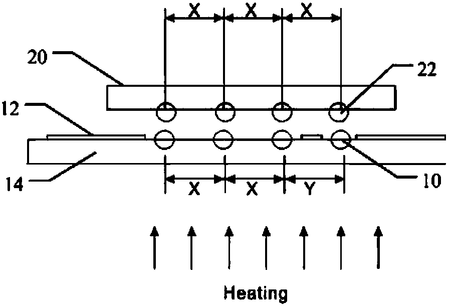
[0026] In the printed circuit board copper cladding method and the copper clad printed circuit board provided by the present invention, during the PCB copper cladding process, a copper cladding prohibition area is set in the soldering area of ​​the BGA package components to prevent the copper skin from being laid under the BGA package components. During the reflow soldering process, the degree of deformation caused by the thermal expansion of the BGA soldering surface of the PCB is reduced, thereby reducing the defective rate of soldering and assembly of BGA package components during the reflow soldering process, and reducing manufacturing costs.

[0027] The following will clearly and completely describe the technical solutions in the embodiments of the present invention with reference to the accompanying drawings in the embodiments of the present invention. Obviously, the described embodiments are only some, not all, embodiments of the present invention. Based on the embodime...


PUM


Abstract

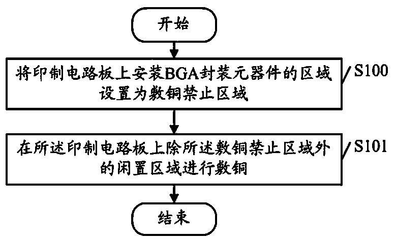
The embodiment of the invention discloses a printed circuit board copper-coating method and a copper-coated printed circuit board. The method comprises the steps of: setting a region on a printed circuit board provided with a ball grid array (BGA) packaged component as a copper-coated prohibited area; and coating copper on regions on the printed circuit board except the copper-coated prohibited area. By implementing the printed circuit board copper-coating method and the copper-coated printed circuit board provided by the invention, in a copper-coating process of the PCB (Printed Circuit Board), the copper-coated prohibited area is set in a welding region of the BGA packaged component so that a copper skin is laid below the BGA packaged component. In a reflow welding process, deformation degree brought to a BGA welding surface of the PCB due to heating expansion is reduced, therefore, reject rate of the welding assembly of the BGA packaged component in the reflow welding process is reduced and manufacture cost is lowered.

Description

technical field [0001] The invention relates to integrated circuit packaging, in particular to a copper-clad printed circuit board method and a copper-clad printed circuit board. Background technique [0002] With the development of electronic technology, electronic products require smaller, faster and more powerful components. As soon as BGA (Ball Grid Array) packaging technology appeared, it became the best choice for high-density, high-performance, multi-pin packaging such as CPU, south / north bridge chip on the motherboard. [0003] BGA packaging technology is to make the pins into balls and arrange them in a grid-like pattern at the bottom of the packaged components. Components packaged with BGA technology can increase the memory capacity by two to three times while maintaining the same volume. BGA packaging technology has greatly improved the storage capacity per square inch. Under the same capacity, the volume of memory products using BGA packaging technology is only...

Claims


Application Information

Patent Timeline
Patent Type & Authority Patents(China)
IPC IPC(8): H05K3/34H05K1/11
Inventor 石裕辉宋盼盼
Owner SHENZHEN SKYWORTH DIGITAL TECH CO LTD
Learn More