Switch, method of manufacturing the same, and electrostatic relay
A manufacturing method and switching technology, which are applied in electrostatic relays/electrical adhesion relays, relays, electrical switches, etc., can solve the problems of difficulty in increasing the thickness of the conductive layer with high hardness and peeling of the conductive layer, and achieve stable contact stability. The effect of increasing the placement area and reducing the wiring resistance
- Summary
- Abstract
- Description
- Claims
- Application Information
AI Technical Summary
Problems solved by technology
Method used
Image

Examples
no. 1 approach
[0067] (structure)
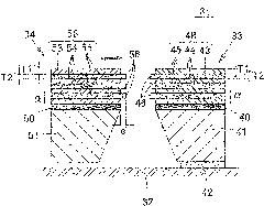
[0068] figure 1 It is a sectional view showing the structure of the switch of Embodiment 1. The switch 31 includes a fixed contact portion 33 and a movable contact portion 34 . The fixed contact portion 33 has its lower surface fixed to the upper surface of the base substrate 32 via the insulating film 42, and the movable contact portion 34 floats from the upper surface of the base substrate 32 and is connected to the base substrate 32 by a driving mechanism or an actuator. Move in the direction parallel to the upper surface (the direction indicated by the white arrow). For example, a MEMS switch having a structure disclosed in Patent Document 1 may be used as the switch of the present invention.
[0069] The fixed contact part 33 is provided with a wiring pattern part 48 on the upper surface of the fixed contact substrate 41 whose surface is covered with the insulating layer 40 . The wiring pattern portion 48 is composed of a base layer 43 located on ...
no. 2 approach
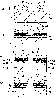
[0104] Figure 7 It is a sectional view showing the structure of a switch 31A according to Embodiment 2 of the present invention. In this switch 31A, without using base layer 43 , buffer layers 44 , 54 and conductive layers 45 , 55 are alternately laminated on the upper surfaces of insulating layer 40 and insulating layer 50 starting from buffer layers 44 , 54 .
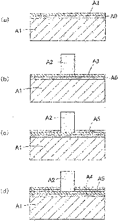
[0105] Figure 8 (a)~(d), Figure 9 (a)~(c) and Figure 10 (a)-(c) are sectional views which show the manufacturing process of switch 31A. In this manufacturing method as well, the wiring pattern portions 48 and 58 are formed by vapor deposition, sputtering, and the like.
[0106] First, if Figure 8 As shown in (a), the upper surface of the substrate A1 is covered with the insulating layer A0, and the buffer layer A4 is formed on the upper surface of the insulating layer A0 by evaporation, sputtering, electroless plating, etc., and then, as Figure 8 As shown in (b), the conductive layer A5 is formed on the up...
no. 3 approach
[0114] Next, the configuration of the high-frequency electrostatic relay 31B according to Embodiment 3 of the present invention will be described. Figure 11 It is a top view showing the structure of the electrostatic relay 31B. Figure 12 will be Figure 11 The enlarged perspective view of part A of Figure 13 It is an enlarged perspective view showing the fixed contact portion 33 and the movable contact portion 34 . Figure 14 is along Figure 11 A schematic cross-sectional view of the B-B line.
[0115] In this electrostatic relay 31B, a fixed contact portion 33 , a movable contact portion 34 , a fixed electrode portion 35 , and a movable contact portion supporting the movable contact portion 34 are provided on the upper surface of a base substrate 32 made of a Si substrate, a glass substrate, or the like. The electrode part 36 , the spring 37 , and the supporting part 38 supporting the spring 37 .
[0116] Such as Figure 14 As shown, the fixed contact part 33 passes...
PUM
| Property | Measurement | Unit |
|---|---|---|
| hardness | aaaaa | aaaaa |
| hardness | aaaaa | aaaaa |
Abstract
Description
Claims
Application Information
 - R&D Engineer
- R&D Manager
- IP Professional
- Industry Leading Data Capabilities
- Powerful AI technology
- Patent DNA Extraction
Browse by: Latest US Patents, China's latest patents, Technical Efficacy Thesaurus, Application Domain, Technology Topic.
© 2024 PatSnap. All rights reserved.Legal|Privacy policy|Modern Slavery Act Transparency Statement|Sitemap