Low-inductance power semiconductor assembly

A technology of power semiconductors and semiconductors, which is applied in the direction of semiconductor devices, electric solid-state devices, electrical components, etc., and can solve problems such as induced voltage spikes

Active Publication Date: 2011-09-21
INFINEON TECH AG
View PDF3 Cites 13 Cited by
  • Summary
  • Abstract
  • Description
  • Claims
  • Application Information

AI Technical Summary

Problems solved by technology

In a similar commutation process, undesired induced voltage spikes are also caused in a corresponding manner in other circuit parts

Method used


Image

  • Low-inductance power semiconductor assembly
  • Low-inductance power semiconductor assembly
  • Low-inductance power semiconductor assembly

Examples


Embodiment Construction

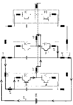
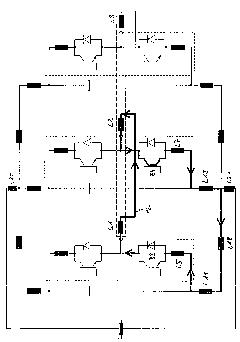
[0047] In the figures, unless otherwise indicated, the same reference numerals denote identical or identically acting elements. Where directional terms are used such as "above", "below", "front", "rear", "front", "rear", etc., these terms relate to the orientation of the corresponding figures. However, the corresponding statements should not be read as limiting. It should be pointed out that the invention can also be realized according to other configurations not shown in the drawings. Furthermore, it should be pointed out that the features of the different exemplary developments described below can be combined with one another, as long as this is not expressly stated otherwise or as long as certain combinations of features are not excluded for technical reasons.

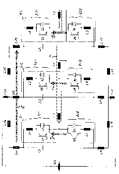
[0048] Figure 4 A first exemplary embodiment of a power semiconductor component according to the invention is illustrated, which in the example shown is realized as a 3-phase converter. The converter comprises t...


PUM


Abstract

The invention relates to a low-inductance power semiconductor assembly. Herein, semiconductor switches employed are arranged in succession in a main current direction.

Description

technical field [0001] The invention relates to a power semiconductor component having two or more bridge branches which each have a phase output for operating an external load. Such a bridge branch can be, for example, a half-bridge branch which generates output potentials, but also a bridge branch which can supply 3 or more potentials at its phase outputs, as in so-called 3-level or multi-level bridge branches. This is the case in the case of step converters. With the aid of such a bridge branch, for example an H-bridge or a multiphase converter can be realized. Background technique [0002] to this end, figure 1 An exemplary circuit diagram of a conventional converter with three half-bridge branches B1, B2 and B3, each having an upper half-bridge branch B1T, B2T and B3T, a lower half-bridge branch B1B, B2B and B3B, and phase output terminals PH1, PH2 and PH3. A common load M, for example a motor, is connected to the phase outputs PH1 , PH2 and PH3 . With respect to t...

Claims


Application Information

Patent Timeline
Patent Type & Authority Applications(China)
IPC IPC(8): H02M1/14H02M1/32H02M7/483
CPCH01L2924/13091H01L25/162H01L2224/48091H02M7/003H01L2224/73265H01L2924/30107H01L2924/13055H01L2924/1305H01L2924/13062H01L2224/49111H01L2224/49175H01L2924/00014H01L2924/00
Inventor R.巴耶雷尔D.多梅斯
Owner INFINEON TECH AG
Why Eureka
Try Eureka