Method for fabricating low resistance, low inductance interconnections in high current semiconductor devices

a technology of flip-chip semiconductors and interconnections, which is applied in the direction of semiconductor devices, semiconductor/solid-state device details, electrical apparatus, etc., can solve the problems of more and more difficult to preserve clean signals without mutual interference, more and more difficult and the cost of interconnection approaches is more expensive than wire bonding, so as to achieve the preservation of clean signals and high reliability, the effect of low electrical resistance and inductan

Active Publication Date: 2008-02-26
TEXAS INSTR INC
View PDF9 Cites 50 Cited by
  • Summary
  • Abstract
  • Description
  • Claims
  • Application Information

AI Technical Summary

Benefits of technology

[0006]Applicants recognize a need to develop a technical approach which considers the complete system consisting of semiconductor chip—device package—external board, in order to provide superior product characteristics, including low electrical resistance and inductance, high reliability, and low cost. Minimum inductance and noise is the prerequisite of high speed, and reduced resistance is the prerequisite of high power. The system-wide method of assembling should also provide mechanical stability and high product reliability, especially in accelerated stress tests (temperature cycling, drop test, etc.). The fabrication method should be flexible enough to be applied for semiconductor product families with shrinking geometries, including substrates and boards, and a wide spectrum of design and process variations.

Problems solved by technology

In addition, there is the relentless pressure to keep the cost / performance ratio under control, which translates often into the drive for lower cost solutions.
Higher levels of integration include the need for higher numbers of signal lines and power lines, yet smaller feature sizes make it more and more difficult to preserve clean signals without mutual interference.
Second, flip-chip assembly often provides higher interconnection densities between chip and package than wire bonding.
These interconnection approaches are more expensive than wire bonding.
In addition, there are severe reliability problems in some stress and life tests of solder ball attached devices.
Furthermore, the higher performance of flip-chip assembled products should be continued even in miniaturized devices, which at present run into severe technical difficulties by using conventional solder ball technologies.

Method used


Image

  • Method for fabricating low resistance, low inductance interconnections in high current semiconductor devices
  • Method for fabricating low resistance, low inductance interconnections in high current semiconductor devices
  • Method for fabricating low resistance, low inductance interconnections in high current semiconductor devices

Examples


Embodiment Construction

[0036]The present invention is related to U.S. patent application Ser. No. 11 / 210,066, filed on Aug. 22, 2005. (Coyle et al., “High Current Semiconductor Device System having Low Resistance and Inductance”; TI-60885).

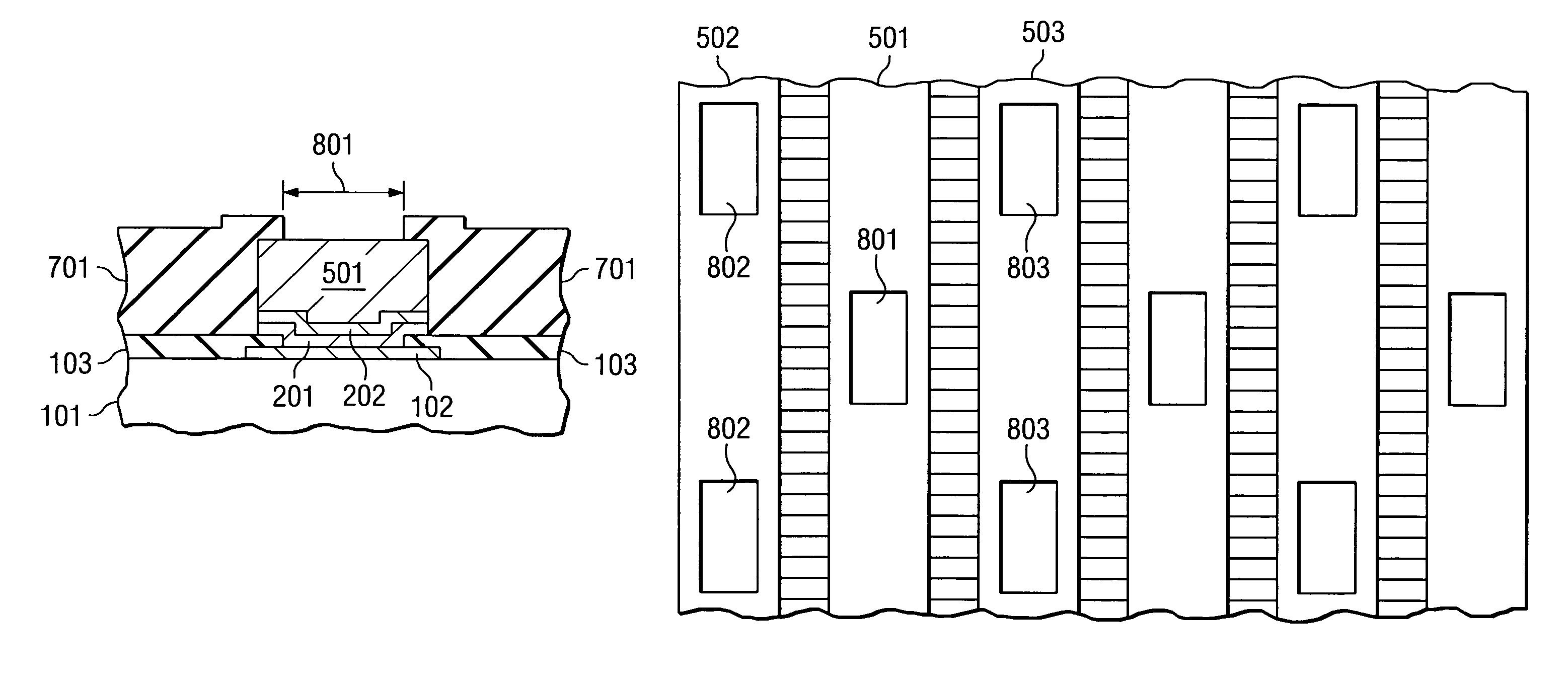
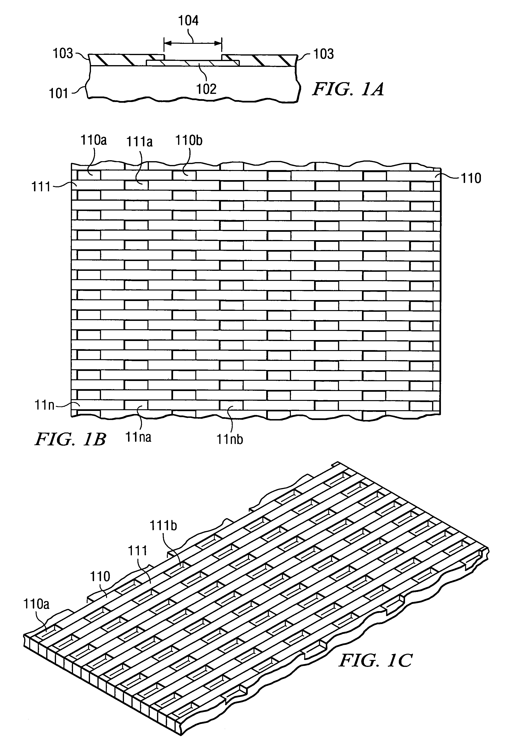
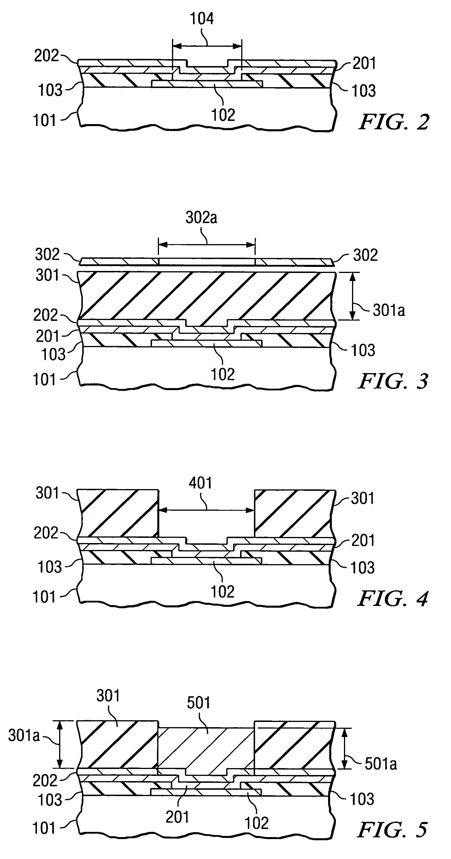
[0037]FIGS. 1A through 15 illustrate certain process steps in the fabrication method of low electrical resistance, low inductance interconnections, which are suitable for high current semiconductor devices and systems. FIG. 1A shows a portion of a semiconductor wafer 101, which has a metallization trace 102 and is protected by an overcoat layer 103. For many devices, the semiconductor wafer is silicon or silicon germanium, but for other devices the wafer may be gallium arsenide or any other compound used in semiconductor product manufacture. The metallization trace for many devices is aluminum or an aluminum alloy, for other devices it is copper or a copper alloy; the thickness range is typically 0.5 to 1 μm. In many devices, the metallization level of trace 102 is the ...


PUM


Abstract

A method for fabricating a low resistance, low inductance device for high current semiconductor flip-chip products. A structure is produced, which comprises a semiconductor chip with metallization traces, copper lines in contact with the traces, and copper bumps located in an orderly and repetitive arrangement on each line so that the bumps of one line are positioned about midway between the corresponding bumps of the neighboring lines. A substrate is provided which has elongated copper leads with first and second surfaces, the leads oriented at right angles to the lines. The first surface of each lead is connected to the corresponding bumps of alternating lines using solder elements. Finally, the assembly is encapsulated in molding compound so that the second lead surfaces remain un-encapsulated.

Description

FIELD OF THE INVENTION[0001]The present invention is related in general to the field of semiconductor devices and processes and more specifically to a fabrication method of high performance flip-chip semiconductor devices, which have low electrical resistance and can provide high power, low noise, and high speed.DESCRIPTION OF THE RELATED ART[0002]Among the ongoing trends in integrated circuit (IC) technology are the drives towards higher integration, shrinking component feature sizes, and higher speed. In addition, there is the relentless pressure to keep the cost / performance ratio under control, which translates often into the drive for lower cost solutions. Higher levels of integration include the need for higher numbers of signal lines and power lines, yet smaller feature sizes make it more and more difficult to preserve clean signals without mutual interference.[0003]These trends and requirements do not only dominate the semiconductor chips, which incorporate the ICs, but also ...

Claims


Application Information

Patent Timeline
Patent Type & Authority Patents(United States)
IPC IPC(8): H01L21/82H01L21/44
CPCH01L24/11H01L23/528H01L23/53238H01L24/05H01L24/13H01L24/14H01L24/16H01L2224/1147H01L2224/13099H01L2924/01013H01L2924/01022H01L2924/01029H01L2924/01032H01L2924/01033H01L2924/01046H01L2924/01047H01L2924/01074H01L2924/01078H01L2924/01079H01L2924/01082H01L2924/10329H01L2924/14H01L2924/19043H01L2924/30107H01L2224/05024H01L2224/14133H01L23/3121H01L2224/02331H01L2224/0235H01L24/03H01L2224/02375H01L2224/0239H01L2224/0345H01L2224/0361H01L2224/05073H01L24/81H01L24/94H01L2224/02313H01L2224/05166H01L2224/05647H01L2224/11462H01L2224/11912H01L2224/13013H01L2224/13082H01L2224/13111H01L2224/13144H01L2224/13147H01L2224/13155H01L2224/13164H01L2224/16225H01L2224/16245H01L2224/81191H01L2224/81424H01L2224/81447H01L2224/8146H01L2224/81815H01L2224/94H01L2924/01006H01L2924/014H01L2924/3841H01L2224/03912H01L2224/02311H01L23/3192H01L2224/0401H01L2924/00014H01L2224/11H01L2224/03H01L2924/01028H01L2224/05193H01L2924/013H01L2924/00H01L2924/181
Inventor LANGE, BERNHARD P.COYLE, ANTHONY L.MAI, QUANG X.
Owner TEXAS INSTR INC
Why Eureka
Try Eureka