Level shift circuit
A technology for converting circuits and levels, applied in the direction of logic circuit connection/interface layout, logic circuit coupling/interface using field effect transistors, etc., can solve the problems of small circuit delay, large circuit delay, logic errors, etc. Effects of delay and response speed
- Summary
- Abstract
- Description
- Claims
- Application Information
AI Technical Summary
Problems solved by technology
Method used
Image

Examples
Embodiment Construction
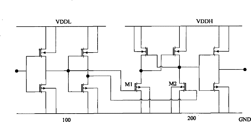
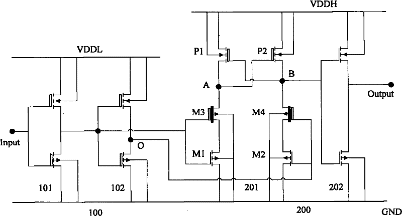
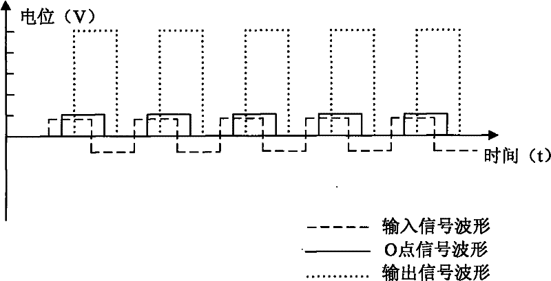
[0022] In the prior art, the first-stage inverter unit of the output circuit is a CMOS mirror inverter circuit, in which each transistor adopts thick-gate transistors in order to meet the withstand voltage requirements of the high operating voltage of the high-level line VDDH . However, when the highest level of the signal output by the shaping circuit is only VDDL, it may cause the problem that the NMOS transistor pair whose gate is connected to the previous stage is difficult to turn on and conduct due to insufficient gate voltage. In the present invention, the NMOS transistor of the first-stage inverter unit of the above-mentioned output circuit is selected as a thin-gate transistor, and a depletion-type thick-gate NMOS transistor pair is added in series with it to play a role of voltage division protection and improve The turn-on speed of NMOS transistors reduces circuit delay.
[0023] The level conversion circuit provided by the present invention is used to convert a hi...
PUM
 Abstract
Description
Claims
Application Information
 - R&D Engineer
- R&D Manager
- IP Professional
- Industry Leading Data Capabilities
- Powerful AI technology
- Patent DNA Extraction
Browse by: Latest US Patents, China's latest patents, Technical Efficacy Thesaurus, Application Domain, Technology Topic.
© 2024 PatSnap. All rights reserved.Legal|Privacy policy|Modern Slavery Act Transparency Statement|Sitemap