Method for reducing latency in a solid-state memory system while maintaining data integrity

a solid-state memory and data integrity technology, applied in the field of reducing latency in solid-state memory systems while maintaining data integrity, can solve the problems of nand flash being faster and more reliable than nand flash, prone to degradation of flash memory, and shortening its lifespan, so as to achieve high fault tolerance, low energy consumption, and fast access

Active Publication Date: 2014-02-25
DATADIRECT NETWORKS
View PDF7 Cites 202 Cited by
  • Summary
  • Abstract
  • Description
  • Claims
  • Application Information

AI Technical Summary

Benefits of technology

[0044]It is an object of the present invention to provide a fast access an

Problems solved by technology

However, flash memory is prone to degradation which often shortens its lifespan considerably.
NOR flash is faster and more reliable than NAND flash but is more expensive.
NAND flash has higher densities than NOR flash and is significantly cheaper but does not have an operational life as long as the NOR flash.
This gives MLC devices a higher storage density than SLC devices but also may cause them to be more prone to errors and reduce the number of program/erase cycles before the cells wear out.
Flash devices are not 100% reliable and often ship with 1-2% of the cells being defective.
Data in flash cells also degrades over time and is subject to disturbances from external influences such as, for example, temperature.
The most prevalent source of corruption of cell data is “Program disturb”, which may occur when cells not being programmed are disturbed by nearby program operations.
“Read disturb” is also an issue with flash devices.
Although being minor per each operation, this problem may accumulate over time.
Flash cells also may wear out over time since the gate levels trends towards a quiescent level.
The cells also wear out with each “program”/“erase” cycle as excess charge accumulates in the dielectric.
This puts a limit on the lifespan of the flash parts since the cells can no longer be used when either the “program” or “erase” operation fails.
(d) wear leveling may introduce large delays due to reading the entire block, programming to new block, and erasing the old block;
(e) wear out of cells in pages may cause delays when the pages need to be re-mapped.
Flash controllers detect and correct many errors but error correction may not always be possible.
It is clear that the re

Method used


Image

  • Method for reducing latency in a solid-state memory system while maintaining data integrity
  • Method for reducing latency in a solid-state memory system while maintaining data integrity
  • Method for reducing latency in a solid-state memory system while maintaining data integrity

Examples


Embodiment Construction

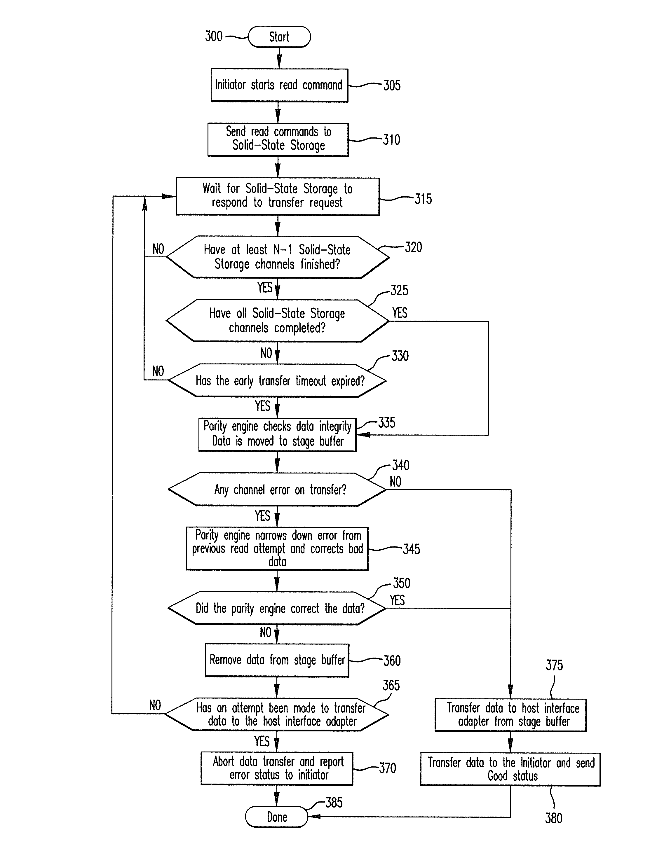
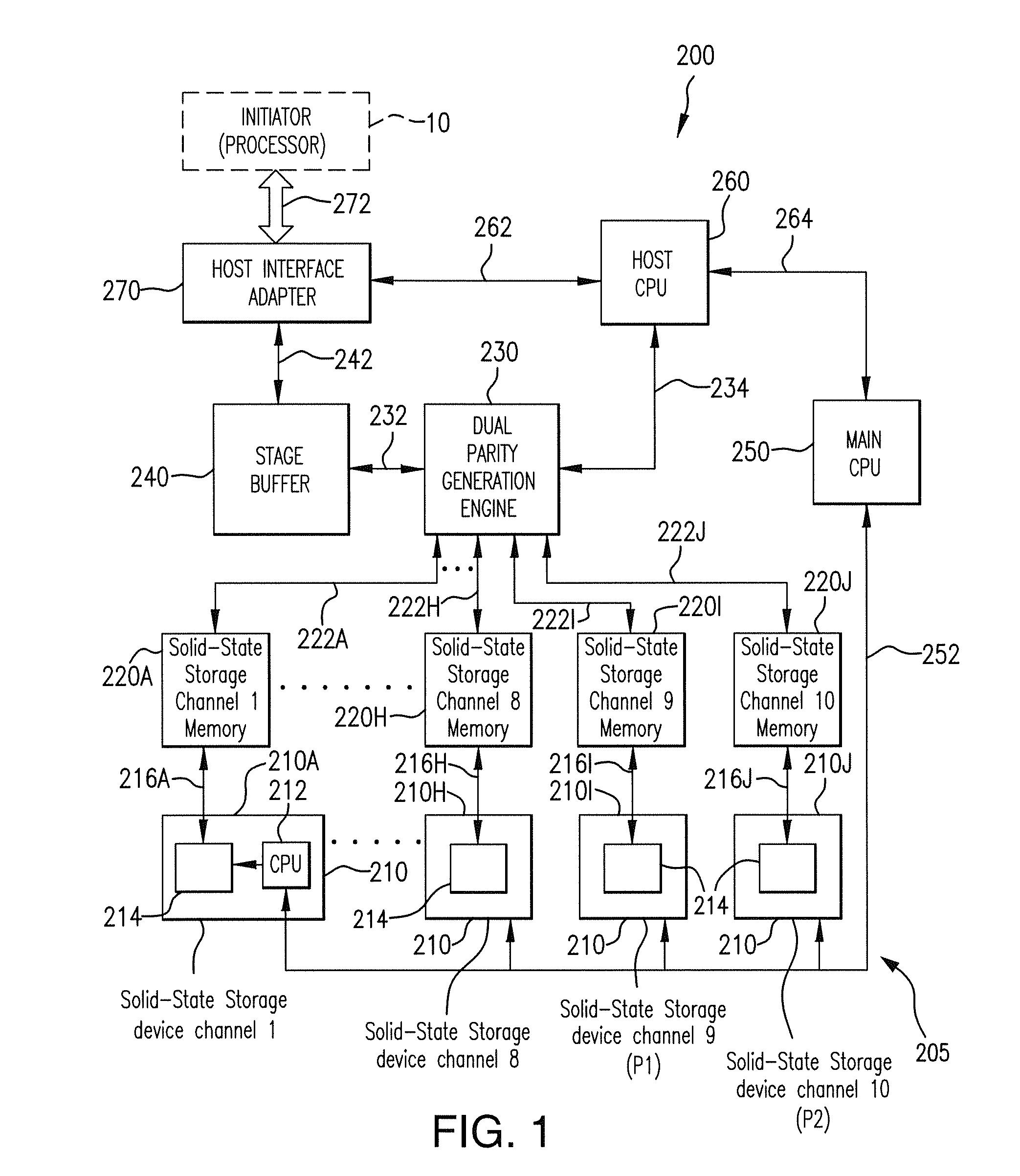
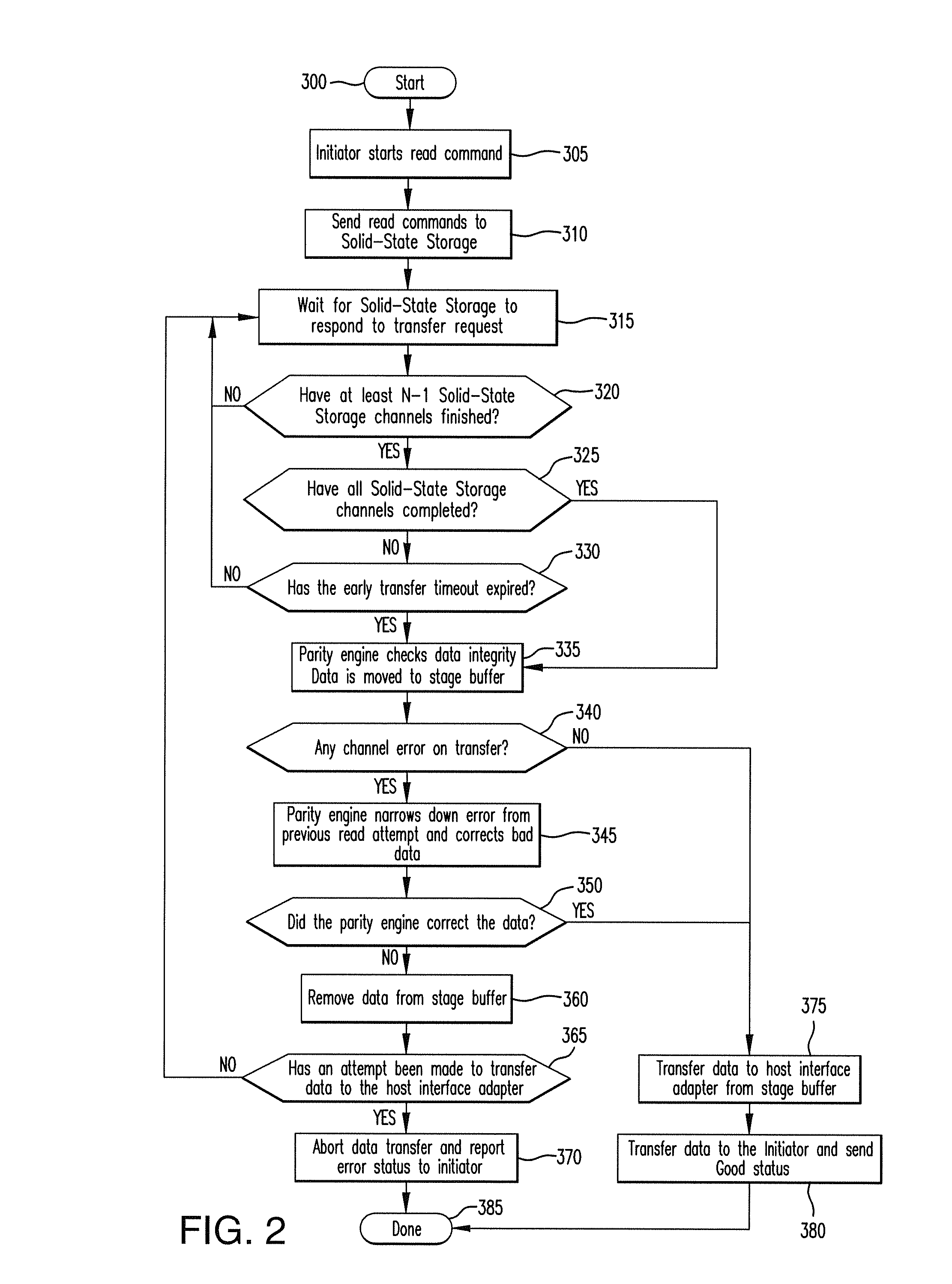
[0055]Referring now to FIG. 1, there is shown memory system 200 for storing and retrieving data for use by one or more processors 10. As will be seen in following paragraphs, memory system 200 provides for access of data with reduced latency while still providing valid data to a requesting processor 10, hereinafter referred to also as an initiator.

[0056]Although not restricted to any particular array of data storage devices, the method of reducing latency while maintaining the integrity of the data stored in memory system 200 is illustrated herein in conjunction with a memory system using a storage array 205 which may be based on a plurality of solid-state storage devices such as, for example, flash memory, or phase-charge memory, as well as memristor memory, or carbon nanotubes memory. The memory system also is contemplated, as an example, as a system having at least two storage devices fault tolerance.

[0057]To have the capability to reduce latency in memory system 200 and maintain...


PUM


Abstract

A latency reduction method for read operations of an array of N solid-state storage devices having n solid-state storage devices for data storage and p solid-state storage devices for storing parity data is provided. Utilizing the parity generation engine fault tolerance for a loss of valid data from at least two of the N solid-state storage devices, the integrity of the data is determined when N−1 of the solid-state storage devices have completed executing a read command. If the data is determined to be valid, the missing data of the Nth solid-state storage device is reconstructed and the data transmitted to the requesting processor. By that arrangement the time necessary for the Nth solid-state storage device to complete execution of the read command is saved, thereby improving the performance of the solid-state memory system.

Description

REFERENCE TO RELATED APPLICATION[0001]The present Patent application is a Continuation-in-Part of the patent application Ser. No. 11 / 907,843 filed on 18 Oct. 2007.FIELD OF THE INVENTION[0002]The present invention is directed to a method for reducing latency in read operations of an array of solid-state storage devices while insuring that valid data is provided therefrom.[0003]More particularly, the present invention is directed to a method of transferring data from less than all of the solid-state storage devices of the array to a stage buffer memory, checking the integrity thereof, and reconstructing the data not transferred if the transferred data is valid.[0004]Still further, the present invention takes advantage of a dual parity generation engine's fault tolerance for a loss of valid data from at least any two of the plurality of solid-state storage devices to transfer and integrity check data from N−1 of N solid-state storage channels to reduce latency of the memory array that ...

Claims


Application Information

Patent Timeline
IPC IPC(8): G06F12/00
CPCG06F2211/1057G06F11/1088G06F11/1076G06F11/108
Inventor PISZCZEK, MICHAELMANNING, J. GORDONFERNANDES, CEDRIC
Owner DATADIRECT NETWORKS
Why Eureka
Try Eureka