
Abrasive, polishing method, method for manufacturing semiconductor integrated circuit device

A grinding method and an integrated circuit technology, which are applied in semiconductor/solid-state device manufacturing, grinding devices, polishing compositions containing abrasives, etc., and can solve the problem of overall complexity of the abrasive supply device, depression, cost and equipment installation space increase and other issues to achieve a high degree of planarization

Active Publication Date: 2014-12-17
AGC INC
View PDF8 Cites 0 Cited by
  • Summary
  • Abstract
  • Description
  • Claims
  • Application Information

AI Technical Summary

Problems solved by technology

However, when using this polishing composition, there is a problem that not only the part to be polished but also the part to be kept is removed by chemical etching, and low-lying parts called dents are likely to occur.
[0007] However, in the polishing method disclosed in Non-Patent Document 1, polishing is performed by combining polishing compositions (abrasives) containing different types of abrasive grains (cerium oxide particles and silica particles), respectively. The overall supply device becomes complicated, and the cost and installation space of the equipment increase
Another problem is that the agglomeration of abrasive grains occurs due to the mixing of two kinds of abrasive grains, and it is easy to cause grinding damage and deterioration of flatness.

Method used


Image

  • Abrasive, polishing method, method for manufacturing semiconductor integrated circuit device
  • Abrasive, polishing method, method for manufacturing semiconductor integrated circuit device
  • Abrasive, polishing method, method for manufacturing semiconductor integrated circuit device

Examples


Embodiment 1~7

[0108] Mix the first grinding agent A and deionized water with a mass ratio of 1:3 (that is, carry out 4-fold dilution with deionized water), and add therein the amount of each ratio shown in Table 2 with respect to the total liquid mass as water-soluble Polyamine pentaethylene hexamine (PEHA). Abrasives (second abrasives) A1 to A7 having pH values ​​shown in Table 2 were thus prepared, respectively.

[0109] Then, using the second abrasives A1 to A7 thus obtained, the above-mentioned objects to be polished (a silicon wafer substrate formed with a silicon dioxide film and a silicon wafer substrate formed with a polysilicon film) were respectively subjected to the grinding pressure shown in Table 3. Polishing was performed for 60 seconds, and the polishing characteristics (polishing speed Vso of the silicon dioxide film and polishing speed Vps of the polysilicon film) were measured respectively. Then, the polishing rate ratio (Vps / Vso) of the polysilicon film and the silicon d...

Embodiment 8

[0111] The mass ratio of 1:9 in Example 8 and the mass ratio of 1:99 in Example 9 were mixed with the first grinding agent A and deionized water, and 0.1% of PEHA was added thereto relative to the total mass of the liquid. Thus, abrasives (second abrasives) A8 and A9 having pH values ​​shown in Table 2 were prepared, respectively.

[0112] Then, using the second abrasives A8 and A9 thus obtained, the above-mentioned objects to be polished (a silicon wafer substrate formed with a silicon dioxide film and a silicon wafer substrate formed with a polysilicon film) were respectively subjected to the grinding pressure shown in Table 3. Polishing was performed for 60 seconds, and the polishing speed Vso of the silicon dioxide film and the polishing speed Vps of the polysilicon film were respectively measured. Then, the polishing rate ratio (Vps / Vso) of the polysilicon film and the silicon dioxide film was calculated from these measured values, respectively. These results are shown i...

Embodiment 10~13

[0114] The first grinding agent A and deionized water were mixed at a mass ratio of 1:3, and polyoxypropylene having a weight average molecular weight (Mw) of 230 as a water-soluble polyamine was added in the ratios shown in Table 2 to the total liquid mass. Diamine (POPD) (manufactured by BASF, trade name, POLYETHERAMINE). Abrasives (second abrasives) A10 to A13 having pH values ​​shown in Table 2 were thus prepared, respectively.

[0115] Then, using the second abrasives A10 to A13 thus obtained, the above-mentioned objects to be polished (a silicon wafer substrate formed with a silicon dioxide film and a silicon wafer substrate formed with a polysilicon film) were subjected to the grinding pressure shown in Table 3, respectively. Polishing was performed for 60 seconds, and the polishing speed Vso of the silicon dioxide film and the polishing speed Vps of the polysilicon film were respectively measured. Then, the polishing rate ratio (Vps / Vso) of the polysilicon film and th...


PUM

PropertyMeasurementUnit
particle sizeaaaaaaaaaa

Abstract

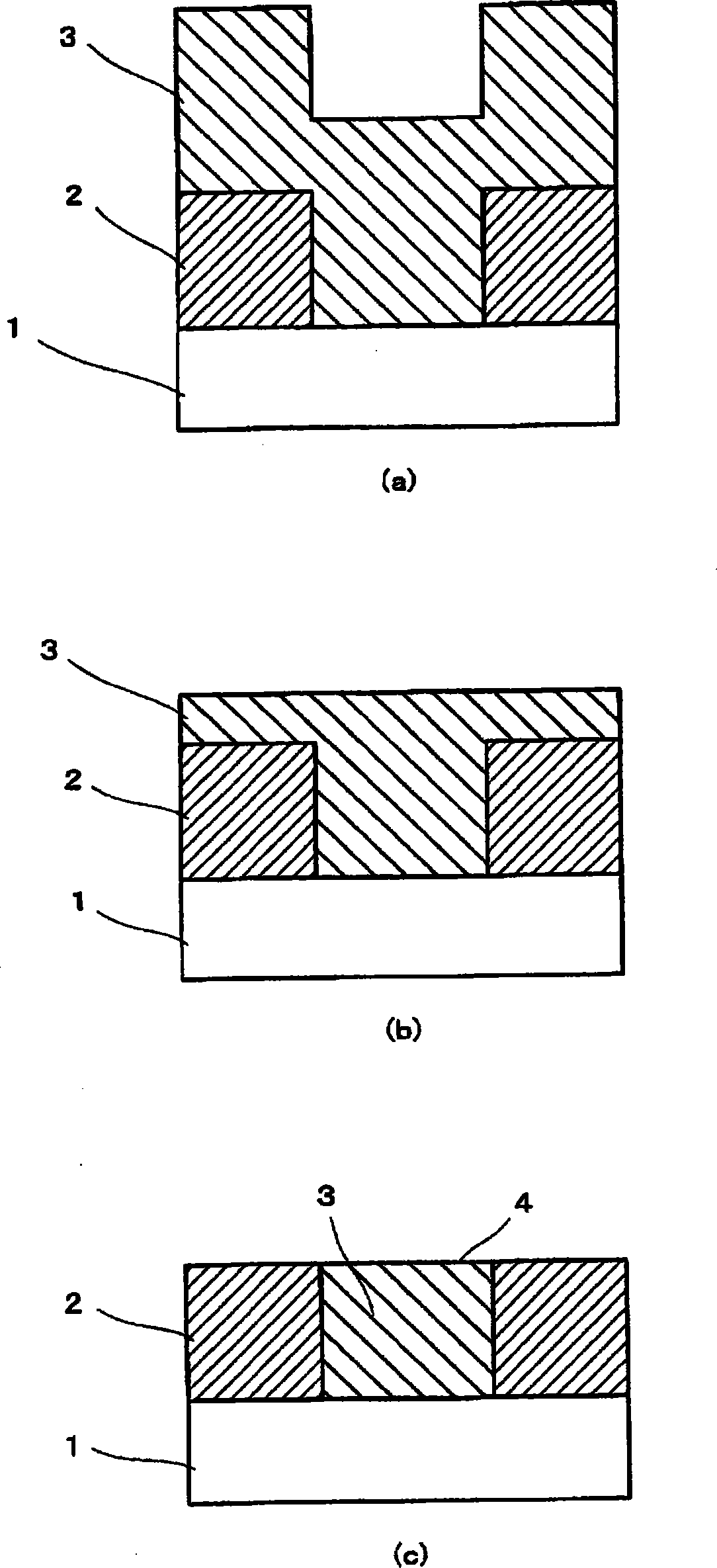
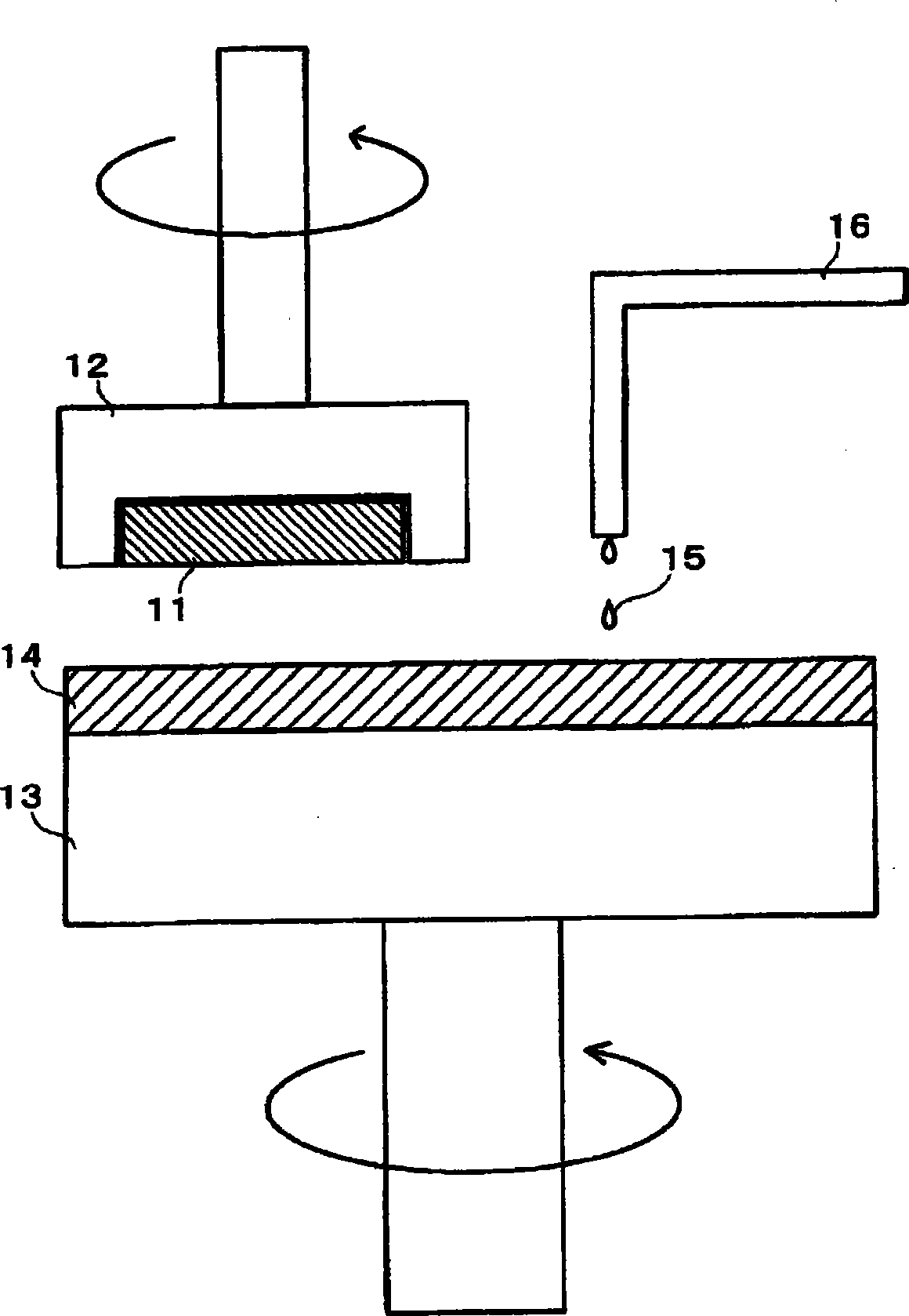
The present invention relates to a polishing method for polishing a to-be-polished surface including a polysilicon film having a silicon dioxide film directly thereunder, in manufacturing a semiconductor integrated circuit device, the method including: a first polishing step of polishing and planarizing the polysilicon film with a first abrasive containing a cerium oxide particle, water and an acid; and a second polishing step of polishing the polysilicon film planarized in the first polishing step with a second abrasive containing at least a cerium oxide particle, water, an acid and a water-soluble polyamine or a salt thereof and stopping polishing by exposure of the silicon dioxide film.

Description

technical field [0001] The present invention relates to an abrasive for chemical mechanical polishing in the manufacture of semiconductor integrated circuit devices, a polishing method, and a method for manufacturing semiconductor integrated circuit devices. More specifically, it relates to an abrasive and a polishing method suitable for flattening a surface to be polished containing a polycrystalline silicon (hereinafter referred to as polysilicon) film, and a method of manufacturing a semiconductor integrated circuit device using the polishing method. The film is used in capacitors, gate electrodes, and the like in a multilayer wiring formation process of a semiconductor integrated circuit device. Background technique [0002] In recent years, along with higher integration and higher functionality of semiconductor integrated circuit devices, the development of microfabrication technologies for miniaturization and higher density of elements has been demanded. In particular...

Claims


Application Information

Patent Timeline
Patent Type & Authority Patents(China)
IPC IPC(8): H01L21/321C09G1/02C09K3/14
CPCC09G1/02H01L21/3212C09K3/1463B24B37/00C09K3/14H01L21/304
Inventor 铃木胜中泽伯人
Owner AGC INC
Learn More