Polishing agent for semiconductor integrated circuit device, polishing method, and method for manufacturing semiconductor integrated circuit device

A technology of integrated circuits and polishing agents, which is applied in the field of polishing, can solve problems such as changes in the polishing rate of silicon nitride films or silicon dioxide films, and achieve a high degree of planarization

Inactive Publication Date: 2009-08-19
ASAHI GLASS CO LTD
View PDF3 Cites 3 Cited by
  • Summary
  • Abstract
  • Description
  • Claims
  • Application Information

AI Technical Summary

Problems solved by technology

[0005] However, there is a problem that when trying to control the polishing rate of the BPSG layer, the polishing rate of the silicon nitride film or silicon dioxide film also varies

Method used


Image

  • Polishing agent for semiconductor integrated circuit device, polishing method, and method for manufacturing semiconductor integrated circuit device
  • Polishing agent for semiconductor integrated circuit device, polishing method, and method for manufacturing semiconductor integrated circuit device
  • Polishing agent for semiconductor integrated circuit device, polishing method, and method for manufacturing semiconductor integrated circuit device

Examples


Embodiment

[0084] Examples of the present invention will be illustrated below. Examples 1 to 4 are examples of the present invention, and examples 5 to 8 are comparative examples. In these examples, "%" means "mass%" unless otherwise specified, and the characteristic values ​​were evaluated in the following ways.

[0085] (pH value)

[0086] The pH was measured with pH81-11 manufactured by Yokogawa Electric Corporation.

[0087] (Average particle size of abrasive grains)

[0088] The average particle diameter was measured by a laser light scattering-diffraction apparatus (trade name LA-920, manufactured by Horiba, Ltd.).

[0089] (dispersion stability of polishing agent)

[0090] The "agglutination and sedimentation time" in the examples was determined based on the time from when 20 mL of the polishing agent was put into a glass test tube with a diameter of 18 mm and allowed to stand for 2 days until separation into two layers occurred to produce a supernatant.

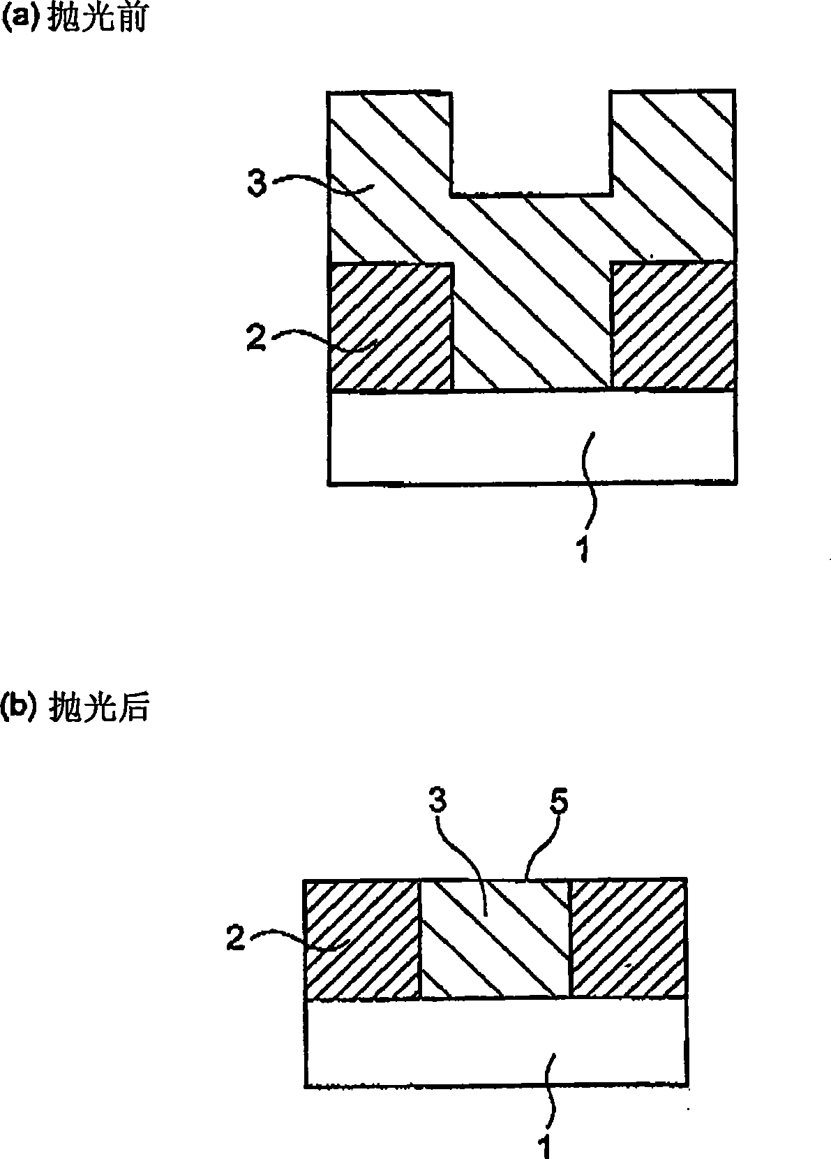
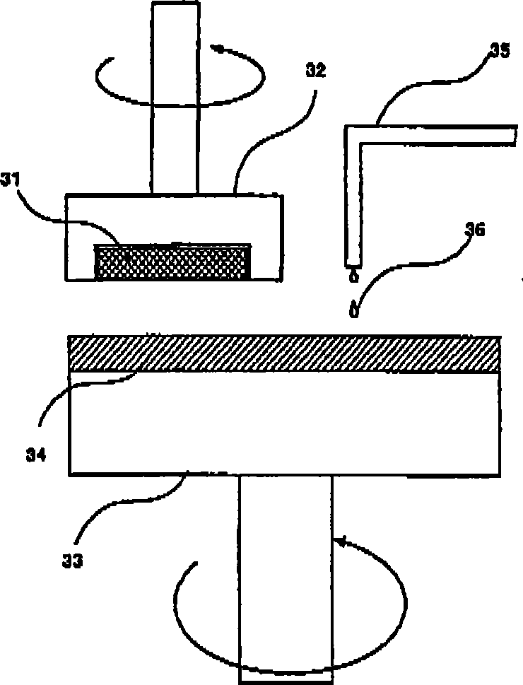
[0091] (Polishing p...

example 1

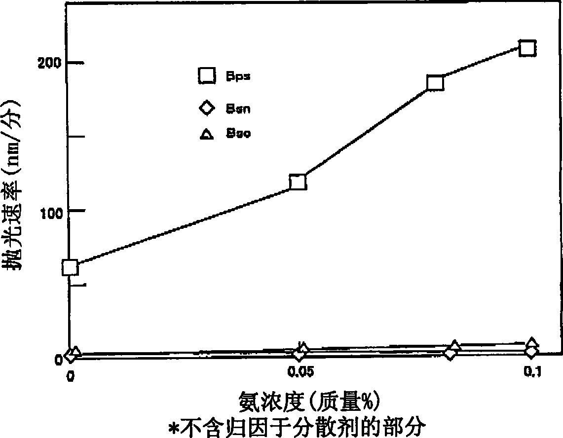
[0106] Stir and mix cerium oxide abrasive grains and ammonium polyacrylate with a molecular weight of 5,000 as a dispersant in deionized water, the mass ratio is 100:0.7, and the mixture is ultrasonically dispersed and filtered to obtain a powder with a concentration of 10% abrasive grains and 0.07% dispersant concentrated mixture. The mixture was diluted 5-fold with deionized water to obtain abrasive mixture A having a concentration of 2.0% abrasive particles and a concentration of 0.014% dispersant. Abrasive mixture A had a pH of 7.6 and an average particle diameter of 0.19 μm.

[0107] Subsequently, polyoxypropylene diamine (amine-based water-soluble polymer, trade name Polyether-Amine, manufactured by BASF) with a molecular weight of 230 as an additive and basic compound ammonia were dissolved in deionized water, thus obtaining Additive solution B1 with polyoxypropylene diamine concentration and 0.1% ammonia concentration.

[0108] Stir and mix additive solution B1 and a...

example 2

[0111]Abrasive mixture A was prepared in the same manner as in Example 1; additive solution B2 was prepared in the same manner as in Example 1 except that the ammonia concentration was adjusted to 0.16% in the preparation of additive solution B1. Additive solution B2 and abrasive grain mixture A are mixed in a mass ratio of 1:1 to obtain a concentration of 1.0% abrasive grains, 0.007% ammonium polyacrylate dispersant concentration, 1.0% polyoxypropylene diamine additive concentration, 0.08% ammonia concentration and Polishing compound with a pH of 10.9.

[0112] The prepared polishing agent was evaluated in the same manner as in Example 1. Table 1 shows the composition of the polishing agent and the evaluation results of polishing performance.


PUM

PropertyMeasurementUnit
particle sizeaaaaaaaaaa

Abstract

The present invention is to provide a polishing technique ensuring that when polishing a to-be-polished surface in the production of a semiconductor integrated circuit device, appropriate polishing rate ratios can be obtained between a borophosphosilicate glass material layer and other materials and high planarization of the to-be-polished surface containing a borophosphosilicate glass material layer can be thereby realized. The present invention relates to a polishing agent for chemical mechanical polishing, containing a cerium oxide particle, a water-soluble polyamine, one or more basic compounds selected from the group consisting of monoethanolamine, ethylethanolamine, diethanolamine and ammonia, and water, wherein the polishing agent has a pH of from 10 to 13 and wherein the basic compound is contained in an amount of more than 0.01 mass%.

Description

technical field [0001] The present invention relates to a polishing technique used in a manufacturing step of a semiconductor integrated circuit device. More specifically, the present invention relates to a polishing agent suitable for planarizing a surface to be polished of a borophosphosilicate glass material layer (hereinafter sometimes referred to as "BPSG layer") used in a semiconductor integrated circuit device, and A technique for polishing a surface to be polished including a BPSG layer in a manufacturing step of a semiconductor integrated circuit device. Background technique [0002] With recent high integration and high functionality of semiconductor integrated circuit devices, the development of microfabrication technology is required to achieve miniaturization and high density. In particular, the importance of planarization technology based on a chemical mechanical polishing method (hereinafter referred to as "CMP") has been rising. [0003] For example, with t...

Claims


Application Information

Patent Timeline
Patent Type & Authority Applications(China)
IPC IPC(8): H01L21/304B24B37/00C09K3/14B24B37/04
CPCC09G1/02B24B37/044H01L21/31053C09K3/1463C09K3/14H01L21/304
Inventor 金喜则吉田伊织中泽伯人
Owner ASAHI GLASS CO LTD
Why Eureka
Try Eureka