Supercharge Your Innovation With Domain-Expert AI Agents!

Optical semiconductor device module

An optical semiconductor element and technology for emitting light, which is applied to optical elements, semiconductor lasers, light guides, etc., can solve the problems of high manufacturing cost, insufficient sealing of optical semiconductor elements, and inability to use plastic lenses, so as to reduce manufacturing costs. Effect

Inactive Publication Date: 2011-10-12
MITSUBISHI ELECTRIC CORP
View PDF9 Cites 0 Cited by
  • Summary
  • Abstract
  • Description
  • Claims
  • Application Information

AI Technical Summary

Problems solved by technology

[0004] However, since the glass lens is expensive, the manufacturing cost of the conventional optical semiconductor element module is high.
On the other hand, there are plastic lenses as low-cost lenses, but plastic lenses cannot sufficiently seal optical semiconductor elements due to their relationship with other materials.
Therefore, low-cost plastic lenses cannot be used in optical semiconductor element modules for optical communications that require sealing.

Method used


Image

  • Optical semiconductor device module
  • Optical semiconductor device module
  • Optical semiconductor device module

Examples


Embodiment approach 1

[0027] figure 1 It is a cross-sectional view showing the optical semiconductor element module of the first embodiment. A semiconductor laser 4 (optical semiconductor element) is mounted on the stem 1 via a heat sink 2 and a sub-fixture 3. A cover 5 is fixed to the stem 1 so as to cover the semiconductor laser 4. A plastic lens 6 and a glass plate 7 are mounted on the cover 5. The plastic lens 6 condenses the emitted light of the semiconductor laser 4. The glass plate 7 seals the semiconductor laser 4.

[0028] In this way, by using the glass plate 7, the semiconductor laser 4 can be sufficiently sealed. In addition, by using the plastic lens 6, the manufacturing cost can be reduced.

[0029] figure 2 It is a cross-sectional view showing a modification of the optical semiconductor element module of the first embodiment. The cover 5 has a mark 8 (guide) at the position where the plastic lens 6 is attached. With this mark 8, the plastic lens 6 can be attached to the cover 5 wit...

Embodiment approach 2

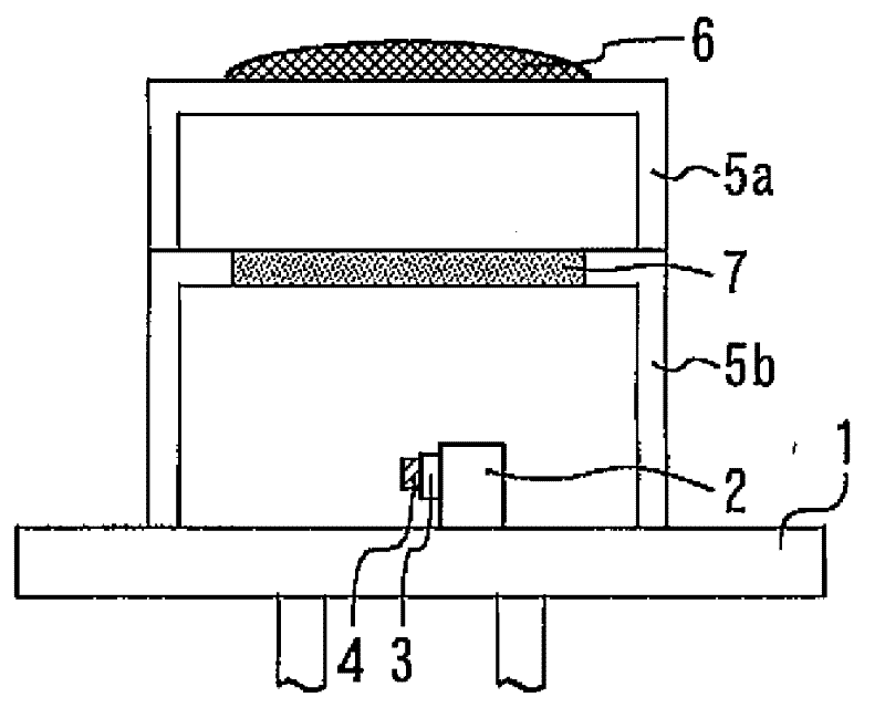
[0031] image 3 It is a cross-sectional view showing the optical semiconductor element module of the second embodiment. The cover 5 a (first cover) to which the plastic lens 6 is mounted and the cover 5 b (second cover) to which the glass plate 7 is mounted are different members. The cover 5a overlaps the cover 5b. Thereby, the cover parts 5a and 5b can be manufactured by the conventional technique.

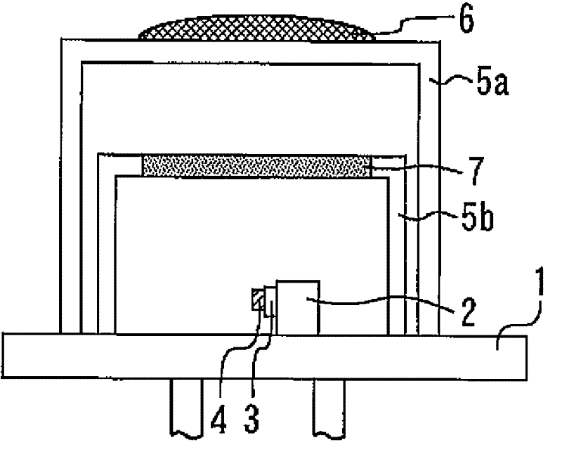
[0032] Figure 4 It is a cross-sectional view showing Modification 1 of the optical semiconductor element module of the second embodiment. In this modification, the cover 5b is overlapped on the cover 5a, and the plastic lens 6 is closer to the semiconductor laser 4 than the glass plate 7 is. Therefore, since the plastic lens 6 is close to the light-emitting part, it is easy to condense light.

[0033] Figure 5 It is a cross-sectional view showing Modification 2 of the optical semiconductor element module of the second embodiment. In this modification, the upper cover part 5a is ...

Embodiment approach 3

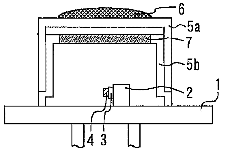
[0035] Image 6 It is a cross-sectional view showing the optical semiconductor element module of the third embodiment. The cover part 5a to which the plastic lens 6 is mounted and the cover part 5b to which the glass plate 7 is mounted are different members. The cover 5a and the cover 5b are respectively fixed to the stem 1. The cover 5a covers the cover 5b. Thereby, the cover parts 5a and 5b can be manufactured by the prior art, and the cover parts 5a and 5b can be fixed to the stem 1 by the prior art.

[0036] Figure 7 It is a cross-sectional view showing a modification of the optical semiconductor element module of the third embodiment. In this modification, the inner wall of the outer cover 5a and the outer wall of the inner cover 5b are in contact. Therefore, if the position of the inner cover part 5b is determined, the position of the outer cover part 5a is automatically determined, so there is no need for positioning.


PUM


Abstract

The present invention relates to an optical semiconductor device module capable of sufficiently sealing an optical semiconductor device and reducing the manufacturing costs. A semiconductor laser 4 is installed on a stem 1. A cover part 5 is fixed on the stem in a way of covering the semiconductor laser 4. A plastic lens 6 and a glass plate 7 are installed on the cover part 5. The plastic lens 6 converges the outcoming light from the semiconductor laser 4. The glass plate 7 seals the semiconductor laser 4. Therefore, the glass plate 7 is used to sufficiently seal the semiconductor laser 4 and the plastic lens 6 is used to reduce the manufacturing costs.

Description

Technical field [0001] The present invention relates to an optical semiconductor element module for optical communication, and particularly relates to an optical semiconductor element module capable of sufficiently sealing the optical semiconductor element and reducing the manufacturing cost. Background technique [0002] In an optical semiconductor element module for optical communication, a lens for condensing light emitted from the optical semiconductor element is attached to a cap. Conventionally, glass lenses have been used as lenses. With this glass lens, both sealing and light focusing of the optical semiconductor element are realized (for example, refer to Patent Document 1). [0003] Patent Document 1: Japanese Patent Application Publication No. 2005-352075. [0004] However, since the glass lens is expensive, the manufacturing cost of the conventional optical semiconductor element module is high. On the other hand, as low-priced lenses, there are plastic lenses, but plas...

Claims


Application Information

Patent Timeline
Patent Type & Authority Applications(China)
IPC IPC(8): G02B6/42
CPCG02B6/4202G02B6/4204H01S5/022
Inventor 田代贺久
Owner MITSUBISHI ELECTRIC CORP
Features
  • R&D
  • Intellectual Property
  • Life Sciences
  • Materials
  • Tech Scout
  • Unparalleled Data Quality
  • Higher Quality Content
  • 60% Fewer Hallucinations
Learn More