Holding table

A workbench and workpiece technology, applied in the direction of electrical components, semiconductor/solid-state device manufacturing, circuits, etc., can solve problems such as unusable, device quality degradation, device damage, etc., to reduce charge, suppress static electricity, and suppress electrostatic damage Effect

Active Publication Date: 2011-10-12
DISCO CORP
View PDF7 Cites 15 Cited by
  • Summary
  • Abstract
  • Description
  • Claims
  • Application Information

AI Technical Summary

Problems solved by technology

[0004] When the wafer is charged, there is a possibility of discharge. When the electricity flowing through the device exceeds the allowable amount due to power generation, electrostatic damage will occur and the device will be damaged. As a result, the quality of the device will be reduced or it will become damaged. can not be used

Method used


Image

  • Holding table
  • Holding table
  • Holding table

Examples


Embodiment Construction

[0027] Next, an embodiment of the present invention will be described.

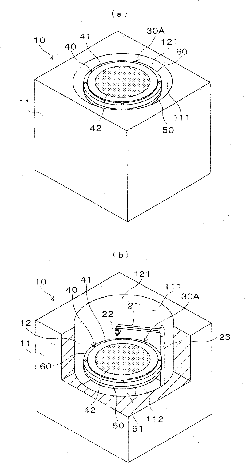
[0028] [1] Cleaning device

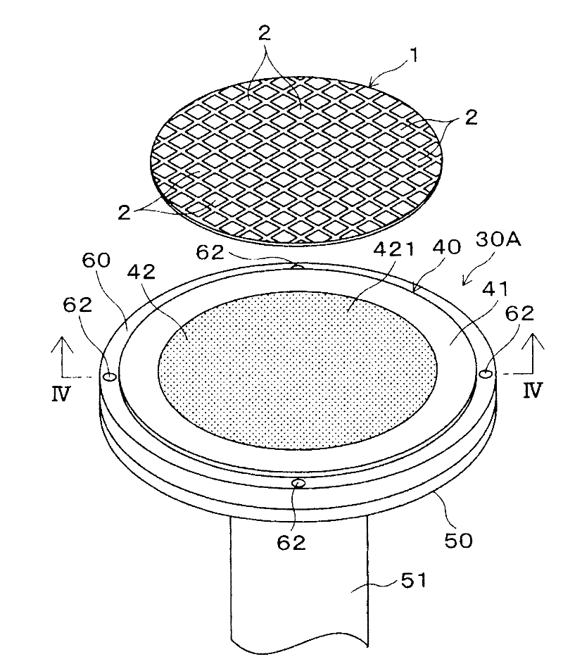
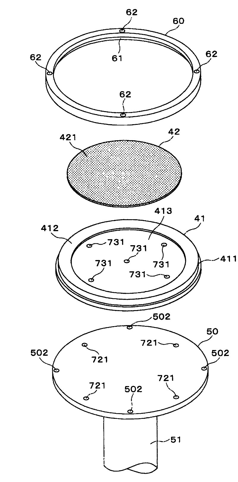
[0029] figure 1 The cleaning device 10 to which the holding table 30A of one embodiment is applied is shown. This cleaning device 10 is preferable as a device for cleaning a thin-plate-shaped workpiece subjected to predetermined processing with a processing device not shown. figure 2 The number 1 of the indicates the artifact here. The workpiece 1 is a disc-shaped semiconductor wafer on the surface of which a large number of rectangular-shaped devices 2 having electronic circuits are formed.

[0030] Examples of processing devices for the workpiece 1 include cutting (scribing) (including cutting with a cutting tool or cutting by laser irradiation), drilling with a laser, grinding, lapping, expanding ( エキスビンド: expand) A processing device such as split processing. The cleaning device 10 of the present embodiment is attached to the processing device described above, or is se...


PUM


Abstract

The invention provides a holding table, wherein the generation of static electricity caused by friction is avoided when workpieces are machined or processed and charges are not easily accumulated in the workpieces so as to reduce the charge amount and suppress the damage caused by static electricity. The holding table comprises a workpiece supporting part (40) equipped with an adsorption part (42) formed by porous bodies and the adsorption part (42) of a frame (41) formed by an insulation body for transmitting negative pressure to the supporting surface (421) of a supporting workpiece (1); a rotation supporting part (50) for supporting the rotation of the workpiece supporting part; a lightweight space (43) formed between the rotation supporting part and the workpiece supporting part; and a suction pathway (70A) for communicating the absorption part with a negative pressure source for generating negative pressure. The suction pathway is not communicated with the lightweight space.

Description

technical field [0001] The present invention relates to a workpiece holding table included in an apparatus for performing various processing and handling on thin-plate workpieces such as semiconductor wafers. Background technique [0002] A large number of rectangular areas are separated by dividing lines on the surface of the semiconductor wafer, and electronic circuits (devices) such as IC (integrated circuit: integrated circuit) or LSI (large-scale integration: large-scale integrated circuit) are formed in this large number of rectangular areas. , and then carry out necessary processing such as grinding and polishing on the back surface of the wafer, and then cut off the planned dividing line to cut (dicing) into individual devices (semiconductor chips), and obtain semiconductor devices through such a process. After the wafers divided into devices are cleaned with a cleaning solution to remove shavings and the like generated during dicing, high-pressure air is sprayed on ...

Claims


Application Information

Patent Timeline
Patent Type & Authority Applications(China)
IPC IPC(8): H01L21/00H01L21/301H01L21/683
Inventor 新田秀次鸟饲刚史瓜田直功山中辅根岸克治
Owner DISCO CORP
Why Eureka
Try Eureka