Method for realizing rapid debugging and locating of chip functional fault and debugging circuit

A technology for functional failure and circuit debugging, applied in electronic circuit testing and other directions, can solve the problems of difficult control of design quality, easy chip damage, high design cost, and achieve fast and low-cost debugging and positioning, and realize the effect of debugging and positioning.

Inactive Publication Date: 2011-11-09
SHANGHAI HUAHONG INTEGRATED CIRCUIT
View PDF6 Cites 8 Cited by
  • Summary
  • Abstract
  • Description
  • Claims
  • Application Information

AI Technical Summary

Problems solved by technology

With the maturity of deep submicron process technology, the chip design industry is facing severe problems: due to the development of chip functions and performance requirements, the chip scale is getting larger, the working speed is getting higher and higher, the development cycle is getting longer and longer, and the design The cost is getting higher and higher, the design quality is becoming more and more difficult to control, the probability of design and production problems after chip production is increasing, and the time and labor costs and complexity of troubleshooting are also increasing
Not only is this method costly and time consuming, but it can easily destroy the chip or introduce other problems in such a small metal pitch

Method used


Image

  • Method for realizing rapid debugging and locating of chip functional fault and debugging circuit
  • Method for realizing rapid debugging and locating of chip functional fault and debugging circuit
  • Method for realizing rapid debugging and locating of chip functional fault and debugging circuit

Examples


Embodiment Construction

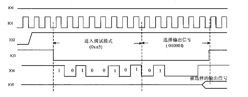
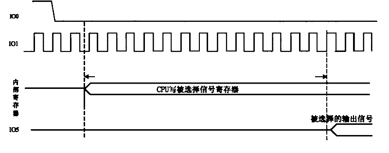
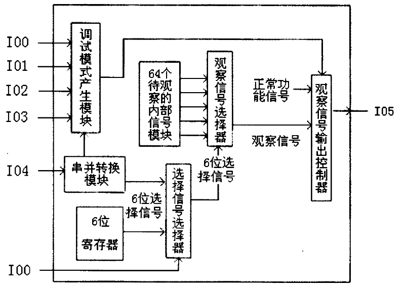
[0012] In one embodiment, the method for quickly debugging and locating chip function faults is to embed a debugging circuit inside the chip during design. When the chip malfunctions, input a predefined signal through one or more pins of the chip to make the chip enter the debugging mode; select the internal signal of the chip to be observed; the selected internal signal of the chip passes through a preset of the chip The defined pins are output; by observing the waveform of some internal signals during the working process of the chip, and comparing it with the expected waveform of the signal during design, the debugging and positioning of functional failures can be realized.

[0013] When the chip malfunctions, there are two ways to select the internal signal of the chip to be observed, which can be selected according to the actual situation of the chip.

[0014] The first way is to input a predefined signal through one or more pins of the chip to make the chip enter the debu...


PUM


Abstract

The invention discloses a method for realizing rapid debugging and locating of a chip functional fault. The method is characterized by comprising the following steps: embedding a debugging circuit in a chip circuit and inputting a predefined signal by virtue of one or more pins of the chip to ensure the chip to enter into a debugging mode when the chip has the functional fault; selecting the internal signals to be observed of the chip; outputting the selected internal signals of the chip by virtue of one predefined pin of the chip; and realizing the debugging and locating of the functional fault by observing the waveforms of certain internal signals in the working process of the chip and comparing the waveforms with the expected waveforms of the signals during design. The invention also discloses the debugging circuit used in the method. By adopting the method, the debugging and locating of the chip fault can be rapidly realized at low cost after the chip has the functional fault.

Description

technical field [0001] The invention relates to the field of chip design, in particular to a method capable of quickly debugging and locating chip function faults. The invention relates to a debugging circuit in the method. Background technique [0002] The development of the semiconductor process level makes it possible to further increase the integration level of integrated circuits (ICs). The electronics industry has entered the VLSI era from the LSI era. With the maturity of deep submicron process technology, the chip design industry is facing severe problems: due to the development of chip function and The cost is getting higher and higher, the design quality is becoming more and more difficult to control, the probability of design and production problems after chip production is increasing, and the time and labor costs and complexity of troubleshooting are also increasing. When designing 3 metal layers ten years ago, if there is a problem with the chip, you can dire...

Claims


Application Information

Patent Timeline
Patent Type & Authority Applications(China)
IPC IPC(8): G01R31/28
Inventor 舒海军
Owner SHANGHAI HUAHONG INTEGRATED CIRCUIT
Why Eureka
Try Eureka