Thimble cap of die bonder

A chip loading machine and thimble technology, applied in electrical components, semiconductor/solid-state device manufacturing, circuits, etc., can solve problems that affect the normal absorption of chips, dicing film gaps, and failure to lock the scribing film, etc., to reduce cracks Or the risk of microcracks, the ejection height of the thimble is reduced, and the effect of vacuum adsorption is firm

Active Publication Date: 2011-11-23
NANTONG FUJITSU MICROELECTRONICS
View PDF5 Cites 6 Cited by
  • Summary
  • Abstract
  • Description
  • Claims
  • Application Information

AI Technical Summary

Problems solved by technology

The surface of the traditional thimble cap is provided with an annular groove, and the scribing film is absorbed by the vacuum of the base part of the equipment and the annular groove on the surface of the thimble cap to prevent the scribing film from being effectively sucked by the vacuum when the thimble is ejected from the ejection hole, resulting in Chip pickup failed
[0003] However, in the actual operation process, there are certain deviations in the viscosity of the scribing film and the vacuum degree of the equipment. Only relying on the existing thimble cap, the vacuum adsorption effect is low, and the scribing film cannot be closely attached to the surface of the thimble cap, resulting in There is a gap between it and the dicing film, and then the vacuum leaks, which fails to achieve the purpose of locking the dicing film, which affects the normal suction of the chip and affects the position accuracy of the chip after loading
Moreover, because the vacuum adsorption is not firm, there will be situations where the ejection height of the thimble is too high and cracks will occur on the back of the chip.

Method used


Image

  • Thimble cap of die bonder
  • Thimble cap of die bonder
  • Thimble cap of die bonder

Examples


Embodiment Construction

[0019] The present invention will be further described below with reference to the accompanying drawings and specific embodiments.

[0020] The invention provides an thimble cap of a chip loading machine.

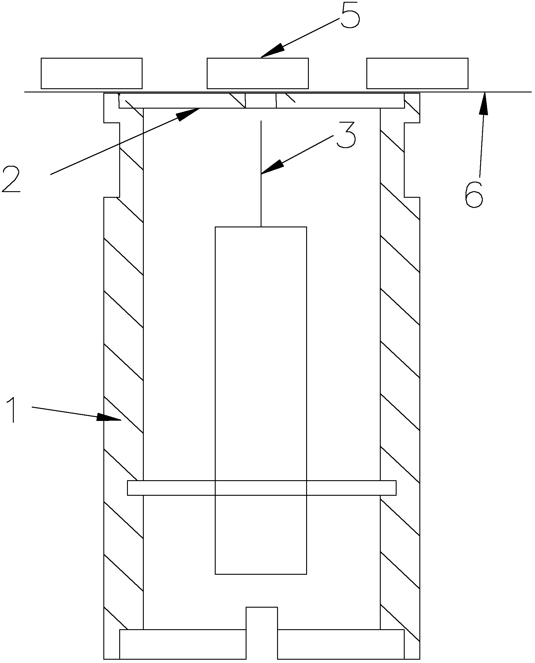
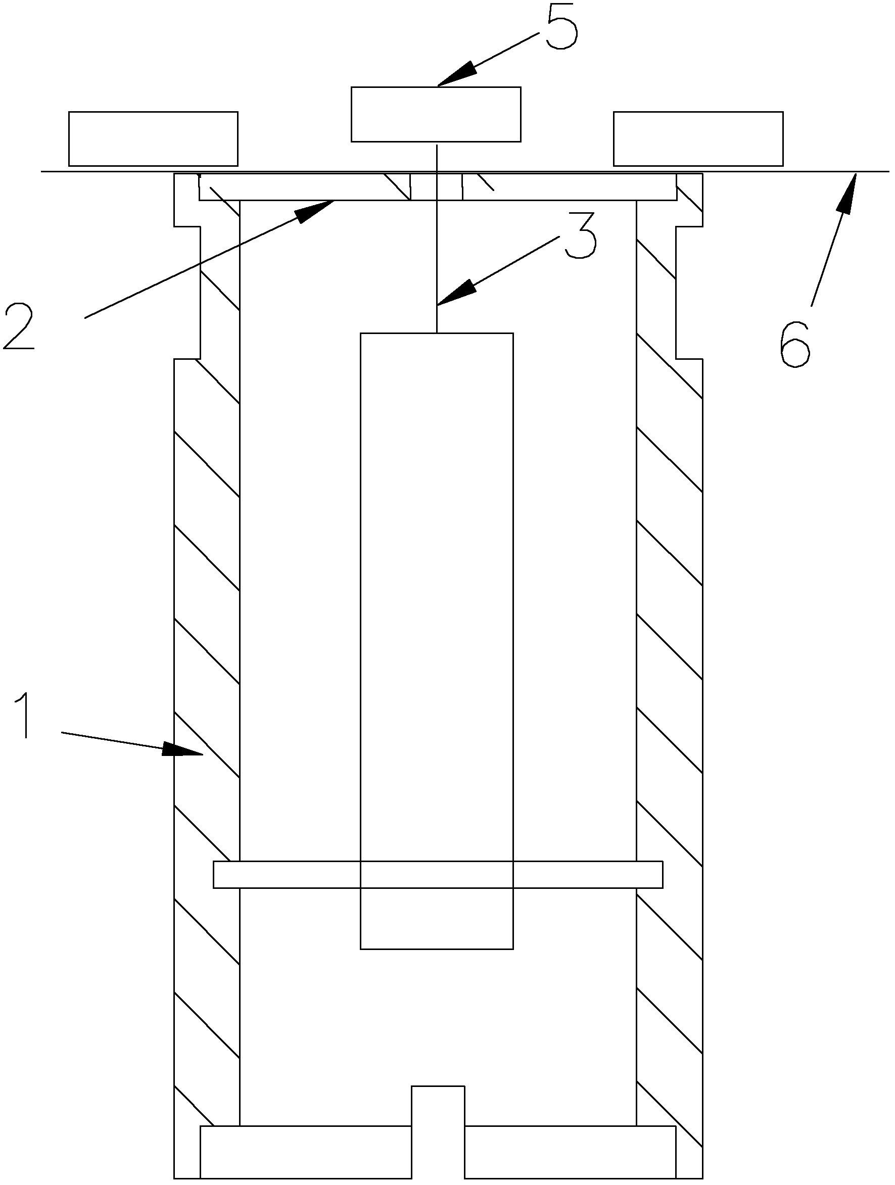
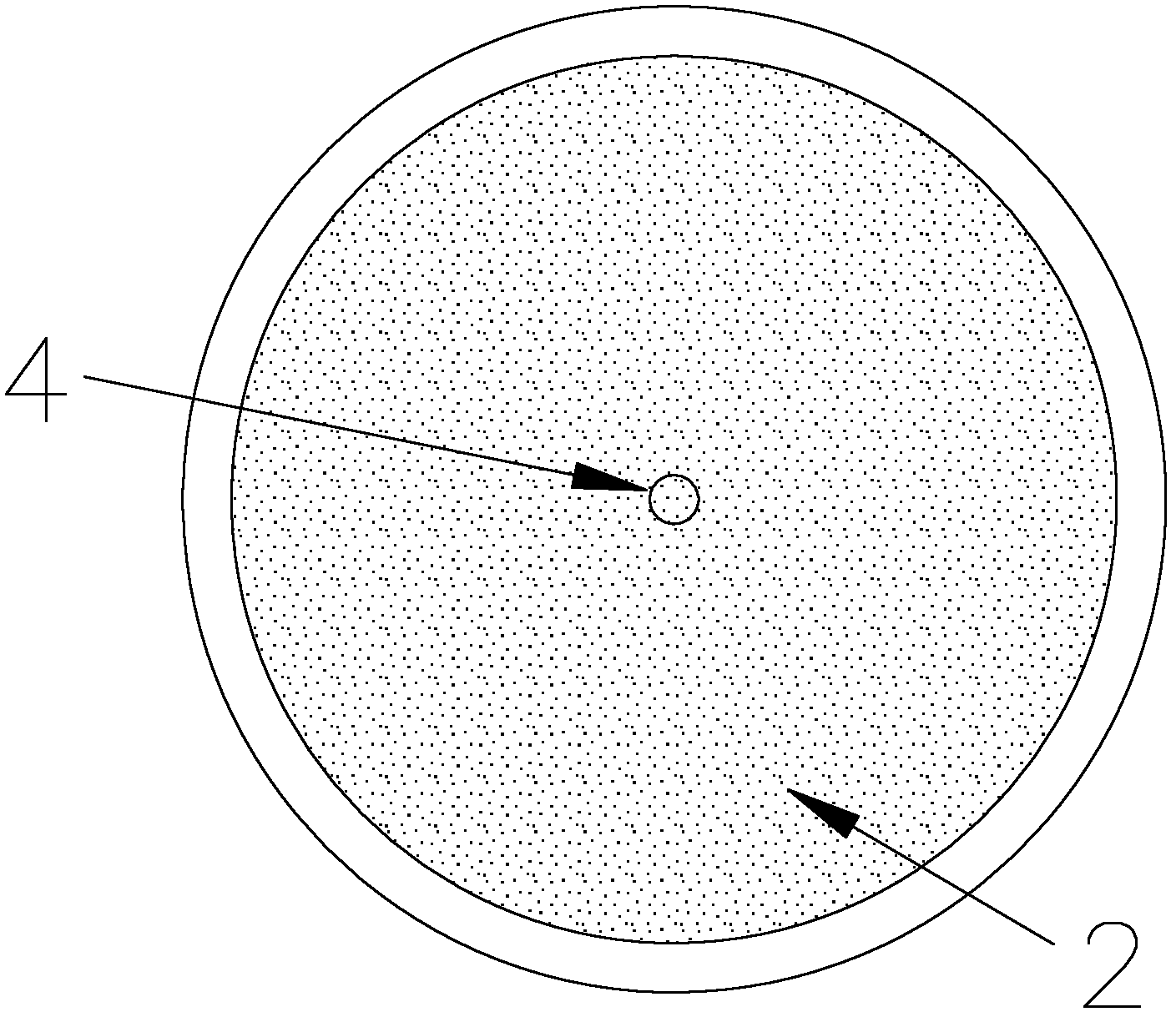
[0021] Such as Figure 1 to Figure 3 Shown: a thimble cap of a film loading machine according to an embodiment of the present invention, including a cap body 1, a cap 2, and an thimble 3 disposed inside the cap body 1, and the cap 2 is made of a porous material.

[0022] As a preferred embodiment of the present invention, the porous material may be, for example, a porous ceramic material, a porous metal material, or the like. The surface of the porous material is smooth, and there are many fine holes distributed inside the material. When the dicing film 6 is attached to the surface of the present invention, the vacuum inside the thimble cap passes through the numerous micropores of the porous ceramic material, and the dicing film 6 Adsorbed on the surface of cap 2.

[00...


PUM


Abstract

The invention relates to a thimble cap of a die bonder. The thimble cap of the die bonder comprises a cap body, a cap cover and a thimble arranged inside the cap body, wherein the cap cover is made of a porous material with micropore, the micropore is used for absorbing a scribing membrane on the cap cover surface, the thimble is one or more, the cap cover is provided with one or more ejection holes for ejecting the corresponding thimbles out of the cap cover, and each ejection hole is arranged on the position of the cap cover opposite to the thimble. According to optimized design and structure of the thimble cap, the thimble cap has the characteristics of simple structure and capability of fully locking a scribing membrane, and has the advantages that the ejection height of a thimble is properly reduced, risks of cracks or micro cracks generated on the back of a chip due to larger ejection height of the thimble is reduced, and the like.

Description

technical field [0001] The invention relates to a film loading device, in particular to an thimble cap of a film loading machine. Background technique [0002] Parts that pick up chips in semiconductor packaging die-loading equipment include thimble caps. The thimble cap is used to absorb the patch film on which the chip is placed. A thimble is arranged inside the cap, which is used to push out the chip to be picked up by a certain distance so that the chip can be picked up. The surface of the traditional thimble cap is provided with an annular groove, and the scribing film is absorbed by the vacuum of the base part of the equipment and the annular groove on the surface of the thimble cap to prevent the scribing film from being effectively sucked by the vacuum when the thimble is ejected from the ejection hole, resulting in Chip pickup failed. [0003] However, in the actual operation process, there are certain deviations in the viscosity of the scribing film and the vacu...

Claims


Application Information

Patent Timeline
Patent Type & Authority Applications(China)
IPC IPC(8): H01L21/687H01L21/50
Inventor 吴斌
Owner NANTONG FUJITSU MICROELECTRONICS
Why Eureka
Try Eureka