Manufacturing process of smooth roughened electrolytic copper foil

A manufacturing process, electrolytic copper foil technology, applied in the field of copper foil manufacturing, can solve the problems of increasing the complexity of copper foil process, product short circuit, open circuit, and increasing processing cost, so as to shorten the production process, reduce short circuit and open circuit rate, The effect of low production cost

Active Publication Date: 2011-12-14
合肥铜冠电子铜箔有限公司
View PDF4 Cites 35 Cited by
  • Summary
  • Abstract
  • Description
  • Claims
  • Application Information

AI Technical Summary

Problems solved by technology

[0002] With the development of electronic information technology, multi-layer complex or high-density thin circuit PCB boards are increasingly used in high-precision miniaturized electronic products. Traditional methods usually use high-precision electronic copper foil or double-sided roughened electrolytic copper foil for high-precision electronic products. Density and thin circuit PCB board or multi-layer complex PCB board inner layer, using traditional high-precision electrolytic copper foil requires complex processes such as micro-etching and blackening after pressing the board, the production process is long and the cost is high; using double-sided roughened electrolytic copper foil It increases the complexity of the copper foil itself and increases the processing cost; secondly, these two kinds of copper foils have the defect of long copper teeth when used in the inner layer of multi-layer boards or high-density thin circuit PCB boards, which is very easy to cause problems for subsequent The product brings major hidden dangers of short circuit and open circuit

Method used


Image

  • Manufacturing process of smooth roughened electrolytic copper foil
  • Manufacturing process of smooth roughened electrolytic copper foil
  • Manufacturing process of smooth roughened electrolytic copper foil

Examples


no. 1 approach

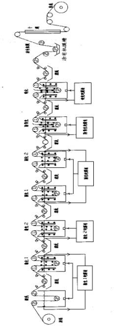
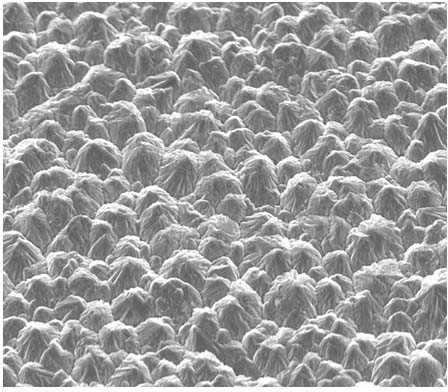
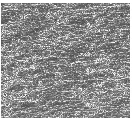
[0020] See figure 1 The first embodiment of the present invention provides the manufacturing process of the roughened electrolytic copper foil (that is, the manufacturing method of the roughened electronic copper foil) is obtained by changing the normal surface treatment method and process of copper foil. The smooth surface is roughened. The production method is to pass the raw foil (unsurface-treated electrolytic copper foil) through the surface treatment equipment, and go through the pickling process, the first step of smoothing, the second step of smoothing, and the smoothing. The first step of curing, the second step of smooth curing, the double-sided anti-oxidation step, the double-sided passivation step, and the smooth coating of coupling agent are completed in a total of eight steps, all of which are concentrated in one surface treatment equipment. The manufacturing method of smooth roughening electronic copper foil uses the raw foil of conventional high-precision electro...

no. 2 approach

[0034] Refer to the manufacturing method of Example 1 to prepare copper foil products. The manufacturing method of the glossy roughened electronic copper foil provided by the second embodiment of the present invention is obtained by changing the normal surface treatment method and process of copper foil. The surface is roughened. The production method is to pass the raw foil (unsurface-treated electrolytic copper foil) through the surface treatment equipment, and go through the pickling process, the first process of smoothing the surface, the second process of smoothing the surface, and the curing of the smooth surface. The first process, the second process of smooth curing, the double-sided anti-oxidation process, the double-sided passivation process, and the smooth coating of coupling agent process are completed in a total of eight consecutive processes, all of which are concentrated in one surface treatment equipment. The manufacturing method of smooth roughening electronic c...

no. 3 approach

[0047] Refer to the manufacturing method of Example 1 to prepare copper foil products. The third embodiment of the present invention provides a method for manufacturing a roughened electronic copper foil by changing the normal surface treatment method and process of copper foil. The surface is roughened. The production method is to pass the raw foil (unsurface-treated electrolytic copper foil) through the surface treatment equipment, and go through the pickling process, the first process of smoothing the surface, the second process of smoothing the surface, and the curing of the smooth surface. The first process, the second process of smooth curing, the double-sided anti-oxidation process, the double-sided passivation process, and the smooth coating of coupling agent process are completed in a total of eight consecutive processes, all of which are concentrated in one surface treatment equipment. The manufacturing method of smooth roughening electronic copper foil uses the raw fo...


PUM


Abstract

The invention relates to a process for manufacturing smooth surface roughened electrolytic copper foil, which comprises a step of pickling, a step of primary smooth surface roughening, a step of secondary smooth surface roughening, a step of primary smooth surface curing, a step of secondary smooth surface curing, a step of double-size anti-oxidization treatment, a step of double side passivation and a step of smooth surface coupling agent treatment, which are accomplished continuously on the same production line. Compared with the prior art, the smooth surface roughened electric copper foil manufactured by the process for manufacturing the smooth surface roughened electrolytic copper foil has the advantages of short copper teeth, easy etching, and high impedance controllability. When the copper foil is used in production of downstream products, the needs of blackening micro corrosion and toughening treatment are obviated, so the manufacturing process is shortened, and the short circuit rate and open circuit rate are lowered; meanwhile, the copper foil manufactured by the process has the same quality as the conventional high-precision or double-side toughened electrolytic copper foil, is produced at low cost and is more suitable for manufacturing the inner layers of high-precision multilayer plates and high-density fine line printed circuit boards (PCBs).

Description

Technical field [0001] The invention relates to a manufacturing method of copper foil, in particular to a manufacturing process of a smooth and roughened electrolytic copper foil. Background technique [0002] With the development of electronic information technology, the use of multi-layer complex or high-density fine circuit PCB boards in high-precision and miniaturized electronic products is increasing. Traditional methods usually use high-precision electronic copper foil or double-sided roughening electrolytic copper foil for high For high-density PCB boards or the inner layers of complex multi-layer PCB boards, the use of traditional high-precision electrolytic copper foil requires complicated processes such as micro-etching and blackening after pressing the board. The production process is long and costly; if double-sided roughening electrolytic copper foil is used The process complexity of the copper foil itself is increased, and the processing cost is increased. Secondly,...

Claims


Application Information

Patent Timeline
Patent Type & Authority Applications(China)
IPC IPC(8): C25D7/06C25D3/38C25D11/34
Inventor 丁士启陆冰沪于君杰朱勇唐海峰郑小伟贾金涛李大双
Owner 合肥铜冠电子铜箔有限公司
Why Eureka
Try Eureka