Defect detection device, defect repair device, defect detection method

A defect detection and defect technology, which is applied in the direction of optical test defects/defects, optics, instruments, etc., to achieve the effects of reducing production costs, shortening production periods, and low costs

Inactive Publication Date: 2011-12-14
SHARP KK
View PDF7 Cites 21 Cited by
  • Summary
  • Abstract
  • Description
  • Claims
  • Application Information

AI Technical Summary

Problems solved by technology

Therefore, even if the defect site candidate includes image elements of multiple colors, it is determined that it is a single color that does not contain multiple color image elements, and the defect site candidate is determined based on the determined single color criterion. Therefore, it becomes judged by standards different from the appropriate judgment standards, and false detection of defects occurs.

Method used


Image

  • Defect detection device, defect repair device, defect detection method
  • Defect detection device, defect repair device, defect detection method
  • Defect detection device, defect repair device, defect detection method

Examples


Embodiment 1

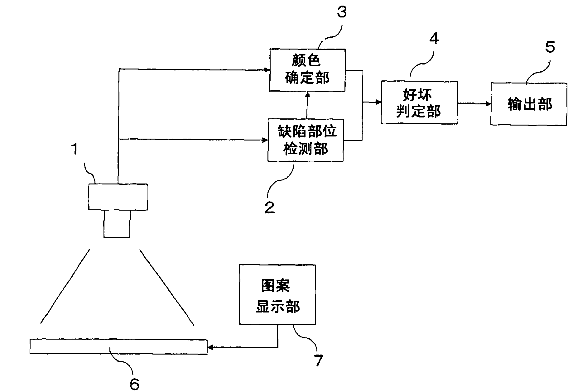
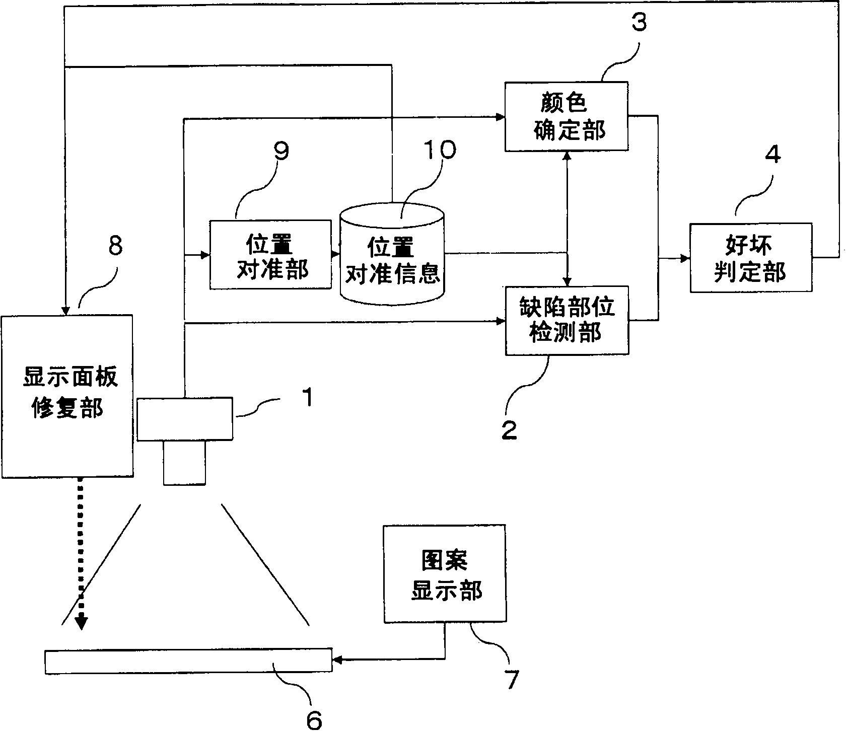
[0047] refer to image 3 , the structure of the defect repairing device according to the embodiment of the present invention will be described. image 3 It is a configuration diagram of a defect repairing device according to the present embodiment and a display device which is an object of defect repairing. The defect repairing device of this embodiment is a device for repairing defects (missing image elements, etc.) of a display device.

[0048] The defect repairing device of this embodiment includes the defect detection device according to this embodiment. Specifically, it includes an imaging unit 1 , a defect detection unit 2 , a color determination unit 3 , and a quality determination unit 4 . Moreover, it is comprised including the display panel repair part 8, the alignment part 9, and the alignment information 10. Moreover, the display device which is the target object of defect detection includes the display panel 6 . The pattern display unit 7 may be included in ei...

Embodiment 2

[0086] The present example is an example in which the calculation method of the step S5 of calculating the degree of defect is different from that of the first example. Other than that, since it is the same as in Example 1, description will be omitted.

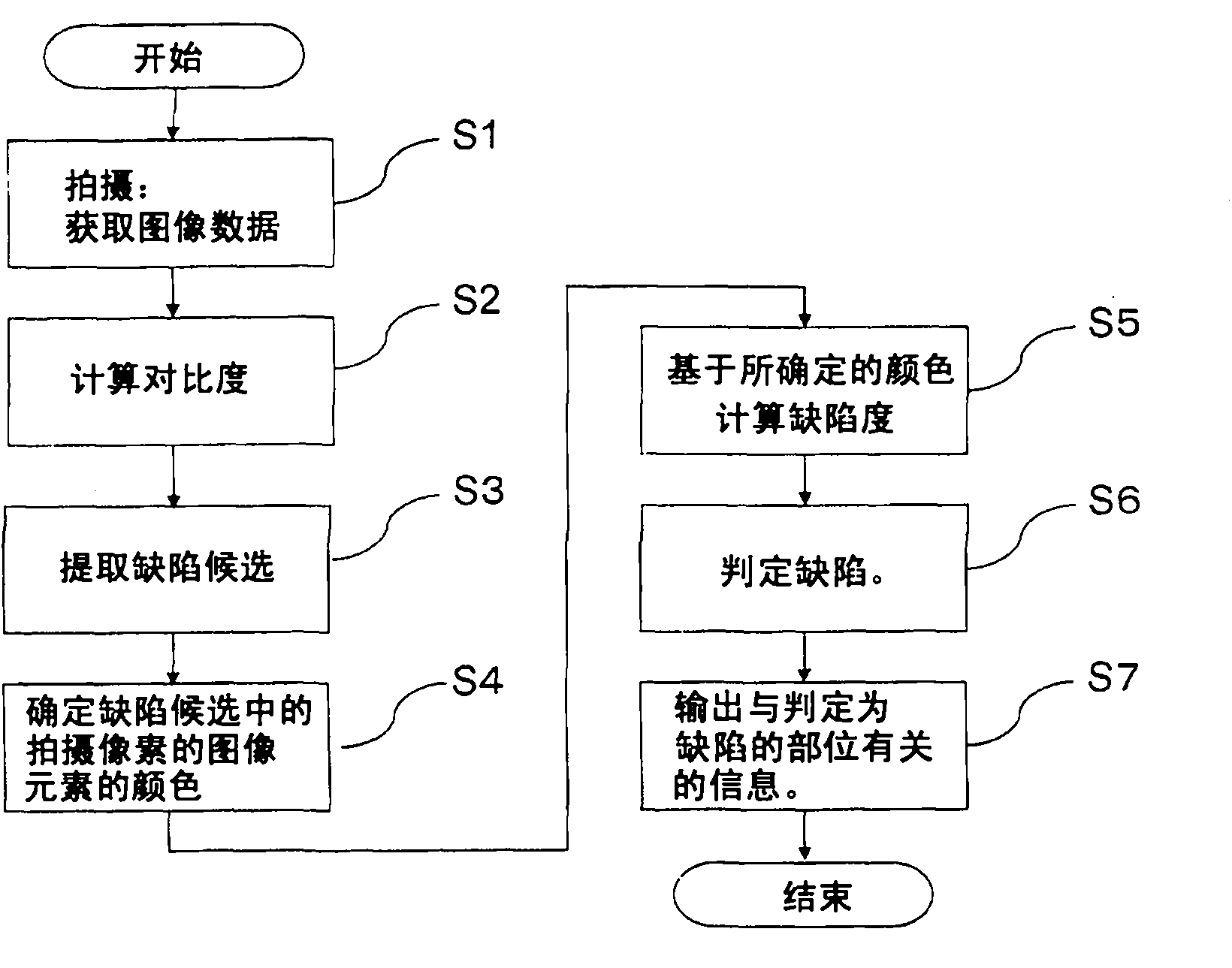
[0087] refer to Figure 9 , and an example of calculation of the defect degree according to the present embodiment will be described. Figure 9 The corresponding relationship between the image element arrangement 100 and the pixel arrangement 101 obtained by photographing the image element arrangement 100 is shown in . The relationship between the picture element arrangement 100 and the pixel arrangement 101 is the same as that of the first embodiment. Furthermore, a contrast value 102a corresponding to the pixel arrangement 101 is shown. The contrast image 102 a is based on image data captured by displaying a solid black pattern on the display panel 6 .

[0088] Figure 9 The contrast value of 102 indicates that one defe...

Embodiment 3

[0106] This embodiment is an embodiment different from the embodiment 1 in the calculation method of the step S4 of specifying the color of the image element of the imaging pixel among the defect candidates. Other than that, since it is the same as in Example 1, description will be omitted.

[0107] use Figure 10 , Step S4 related to this embodiment will be described. In this example, something like Figure 10 Like the color 101a of the pixels x2, x4, x6, x8, and x10 shown, when one pixel includes (corresponds to) two or more image elements, the area ratio of each image element in the pixel is regarded as 1:1.

[0108] Although the method similar to Example 1 was used in the process after process S5, since the color 101a of a pixel differs from Example 1, the defect degree different from Example 1 was calculated.

[0109] by Figure 10 The calculation of the defect degree of x4 shown will be described as an example. First, the contrast value for each color when controll...


PUM


Abstract

The invention discloses a defect detecting device, a defect restoring device and a defect detecting method. The invention provides a defect detecting device which is capable of judging defects in a proper standard according to the color proportion even when the defects contain multiple-color image elements. The defect detecting device comprises a shooting part for shooting a display panel and obtaining image data; a defective part detecting part for selecting defective part candidates from the image data; a color determining part for determining the image element color of the defective part candidates; and a judging part for calculating the defective rate by multiplying a contrast degree with a correction coefficient varying with different colors, and then judging the defects by comparing the defective rate with a judging value. The judging part concludes after the contrast degree and a corresponding correction coefficient of each color are multiplied to calculate the defective rates when a defective part candidate comprises multi-color image elements.

Description

technical field [0001] The present invention relates to a technique for detecting defects of a display panel by capturing an image displayed on a display panel including a plurality of color image elements such as a color LCD panel by using a camera. Background technique [0002] Patent Document 1 discloses a defect inspection device that inspects a display panel for defects by imaging a display panel in which image elements of a plurality of colors are arranged in a certain direction by an imaging unit having an imaging element. [0003] The defect inspection device described in Patent Document 1 includes an image processing unit for determining defects by processing image data captured by an imaging element. The image processing unit includes: a pattern display unit that displays an inspection pattern for inspecting defects of the display panel on the display panel; a defective part detection unit for a defective part candidate; and a defect part color specifying part for...

Claims


Application Information

Patent Timeline
Patent Type & Authority Applications(China)
IPC IPC(8): G01N21/88G02F1/13
Inventor 山本修平中西秀信植木章太
Owner SHARP KK
Why Eureka
Try Eureka