Decomposed circuit interconnection testing method based on boundary scanning technology

A boundary scan and circuit interconnection technology, which is applied in the direction of electronic circuit testing, electrical measurement, measuring devices, etc., can solve the problem of low accuracy of fault diagnosis, achieve improved reliability and feasibility, reduce difficulty, and achieve high accuracy Effect

Inactive Publication Date: 2013-11-06
HARBIN INST OF TECH
View PDF6 Cites 0 Cited by
  • Summary
  • Abstract
  • Description
  • Claims
  • Application Information

AI Technical Summary

Problems solved by technology

[0004] The present invention aims to solve the problem of low accuracy of fault diagnosis in the existing circuit interconnection test method, thereby providing a decomposed circuit interconnection test method based on boundary scan technology

Method used


Image

  • Decomposed circuit interconnection testing method based on boundary scanning technology
  • Decomposed circuit interconnection testing method based on boundary scanning technology
  • Decomposed circuit interconnection testing method based on boundary scanning technology

Examples


specific Embodiment approach 1

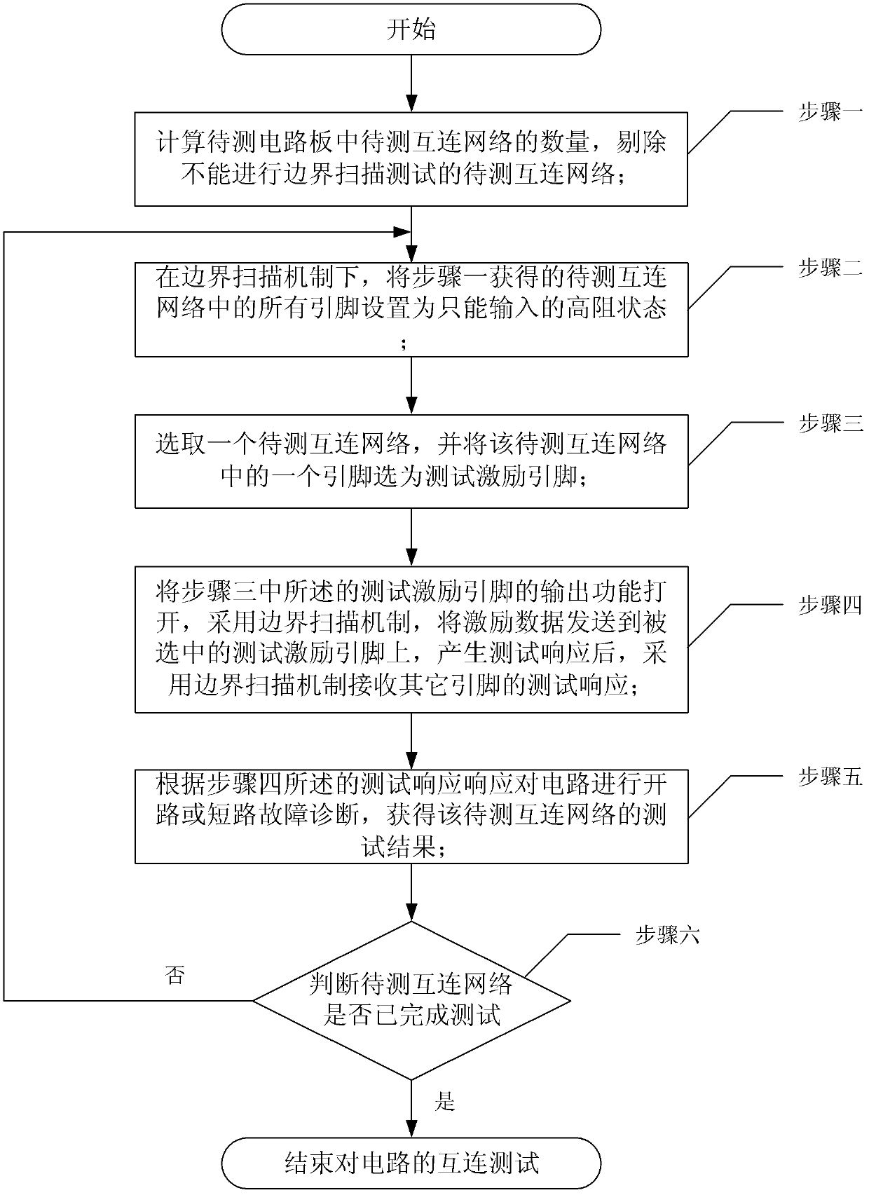
[0015] Specific implementation mode 1. Combination figure 1 Illustrate this specific embodiment, a kind of decomposed circuit interconnection test method based on boundary scan technology, it is realized by the following steps:

[0016] Step 1, calculating the number of interconnection networks to be tested in the circuit board to be tested, and eliminating the interconnection networks to be tested that cannot be tested by boundary scan;

[0017] Step 2. Under the boundary scan mechanism, set all pins in the interconnection network to be tested obtained in step 1 to a high-impedance state that can only be input;

[0018] Step 3, select an interconnection network to be tested, and select a pin in the interconnection network to be tested as a test excitation pin, and generate data '1' or '0';

[0019] Step 4. Turn on the output function of the test stimulus pin described in step 3, and use the boundary scan mechanism to send the stimulus data to the selected test stimulus pin. ...

specific Embodiment approach 2

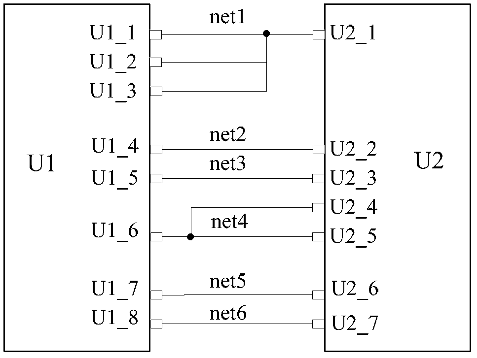
[0024] Specific Embodiment 2. In this specific embodiment, a circuit interconnection is taken as an example to describe the method of the present invention; figure 2 As shown, the interconnected chips are U1 and U2, and there are 6 measurable interconnection networks: net1 to net6. The specific test process is as follows:

[0025] Step 1, calculating the number of interconnection networks to be tested in the circuit board to be tested, and eliminating the interconnection networks to be tested that cannot be tested by boundary scan;

[0026] Specifically: According to the circuit schematic file (.net file), find the interconnection network in the circuit, and remove the network that cannot be controlled by the boundary scan mechanism, and the remaining network number is the total number of measurable networks.

[0027] Step 2. Under the boundary scan mechanism, set all the pins in the interconnection network to be tested that are eliminated in step 1 to a high-impedance state ...


PUM


Abstract

The invention discloses a decomposed circuit interconnection testing method based on a boundary scanning technology, which relates to a circuit interconnection testing method and is used for solving the problem of low fault diagnosis accuracy of the conventional circuit interconnection testing method. The method comprises the following steps of: selecting an interconnection network to be tested, selecting a pin of the interconnection network to be tested serving as a testing excitation pin, switching on the output function of the testing excitation pin, transmitting excitation data to the selected testing excitation pin by adopting a boundary scanning mechanism, and receiving testing responses of other pins by adopting the boundary scanning mechanism after a testing response is made; and diagnosing the open circuit or short circuit fault of a circuit according to the testing response to obtain a testing result of the interconnection network to be tested. The method is suitable for circuit interconnection testing.

Description

technical field [0001] The invention relates to a circuit interconnection testing method. Background technique [0002] With the rapid development of electronic technology, large-scale integrated circuits and complex digital chips are more and more widely used in electronic equipment, which makes the testing of circuit boards increasingly difficult, especially after the emergence of surface mount (SMT) technology, The mounting density of devices on the circuit board is getting higher and higher, and the distance between the nodes available for testing is getting smaller and smaller, and some even completely become recessive unreachable nodes. Traditional testing methods such as bed of needles and probes are already very It is difficult to effectively test the interconnection of the circuit board (interconnection of circuit nodes). [0003] When using boundary-scan technology for interconnection testing, the test algorithm is a key link. Traditional test algorithm (such as:...

Claims


Application Information

Patent Timeline
Patent Type & Authority Patents(China)
IPC IPC(8): G01R31/28G01R31/02
Inventor 朱敏刘思久杨春玲陈宇杨江李洋
Owner HARBIN INST OF TECH
Why Eureka
Try Eureka