Display device, projection device, near-eye display device and method for forming same

A display device and plane technology, applied in projection devices, optics, instruments, etc., can solve the problems of reduced size and volume, disadvantage, complex optical system of projection devices, etc., and achieve the effect of high light modulation and display, high resolution

Active Publication Date: 2011-12-14
XIAN YISHEN OPTOELECTRONICS TECH CO LTD
View PDF5 Cites 11 Cited by
  • Summary
  • Abstract
  • Description
  • Claims
  • Application Information

AI Technical Summary

Problems solved by technology

[0006] The problem solved by the present invention is that the optical system of the projection device in the prior art is complicated, which is not conducive to reducing the size and volume

Method used


Image

  • Display device, projection device, near-eye display device and method for forming same
  • Display device, projection device, near-eye display device and method for forming same
  • Display device, projection device, near-eye display device and method for forming same

Examples


Embodiment Construction

[0083] In order to enable those skilled in the art to better understand the present invention, the display device of the present invention will be described in detail below with reference to the drawings and specific embodiments.

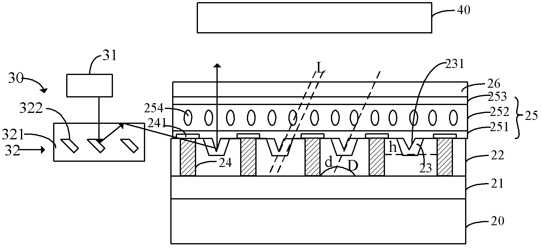
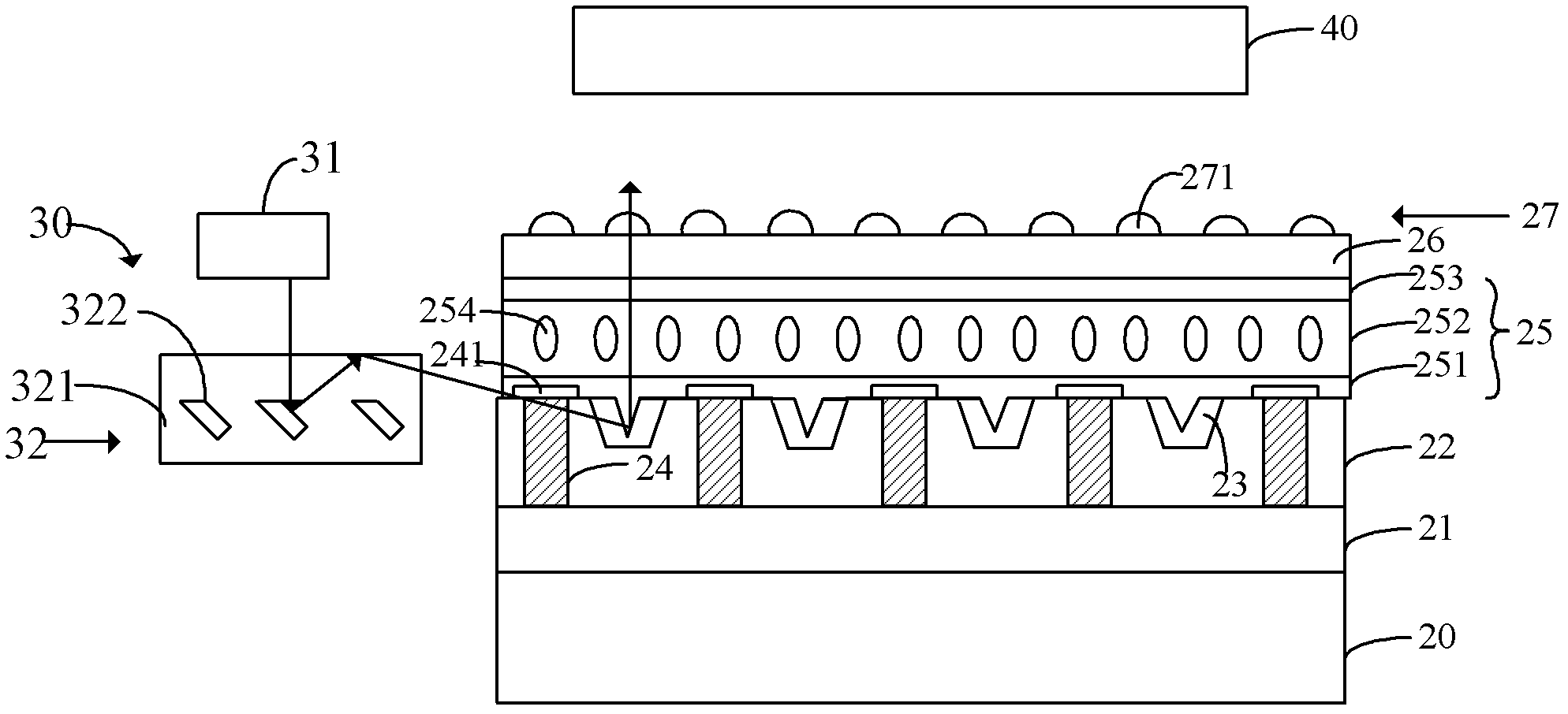
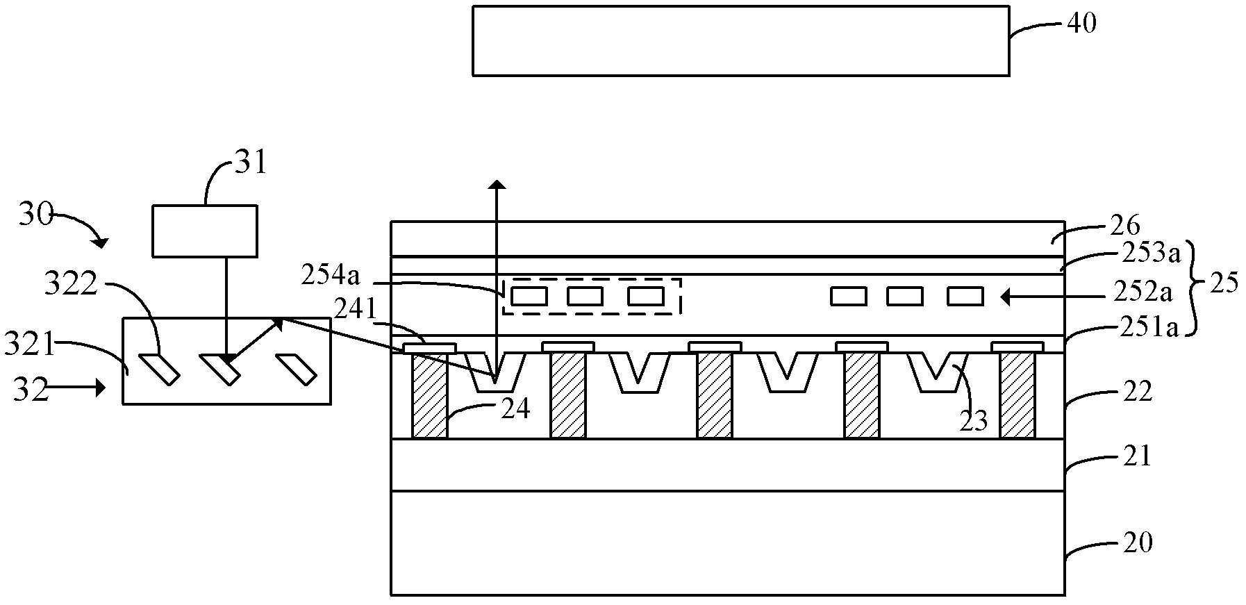
[0084] refer to figure 1 , the display device of the first specific embodiment of the present invention includes: a substrate 20, a semiconductor switch array 21 located on the substrate 20; a planar light guide plate located on the semiconductor switch array 21, and the planar light guide plate includes a transparent The dielectric layer 22, the optical path deflection micro-device and the electrical connector located in the transparent dielectric layer 22, the electrical connector is electrically connected with the semiconductor switch array 21; it is located on the planar light guide plate, that is, on the transparent dielectric layer 22 The transmission light valve array 25, the transmission light valve array 25 has a plurality of transmission ...


PUM

PropertyMeasurementUnit
thicknessaaaaaaaaaa
thicknessaaaaaaaaaa
thicknessaaaaaaaaaa

Abstract

The invention discloses a display device, a projection device and a near sight display device and a forming method thereof. The display device comprises a substrate, a semiconductor switch array, a plane light guide panel and a transmission light valve array, wherein the semiconductor switch array is positioned on the substrate; the plane light guide panel is positioned on the semiconductor switch array and comprises a transparent medium layer, and a light path deflection micro device and an electrical connector which are positioned in the transparent medium layer; the electrical connector iselectrically connected with the semiconductor switch array; the transmission light valve array is positioned on the plane light guide panel and is provided with a plurality of transmission light valves which are arranged to form an array; the electrical connector is also electrically connected with the transmission light valve array; the semiconductor switch array controls the opening and the closing of the transmission light valves by the electrical connector; light which is transmitted from the side of the plane light guide panel to the plane light guide panel is deflected by the light pathdeflection micro device, transmitted to the transmission light valve array and transmitted to the outside after passing through the transmission light valve array. Light modulation and display with high resolution can be realized in a limited area, and the display device is a novel transmission type micro display chip.

Description

technical field [0001] The present invention relates to the display field, in particular to a display device, a projection device, a near-eye display device and a forming method thereof. Background technique [0002] In the projection system, according to different projection principles, it can be divided into reflective projection system and transmissive projection system. Reflective projection system mainly includes: digital light processing projection display system (DLP projection display system) and liquid crystal on silicon projection display system (LCOS projection display system) . The transmissive projection system is mainly a liquid crystal display projection display system (LCD projection display system). [0003] DLP projection display system is divided into single-chip DLP projection display system and three-chip DLP projection display system, Figure 16 It is a structural schematic diagram of a three-chip DLP projection display system in the prior art, refer ...

Claims


Application Information

Patent Timeline
Patent Type & Authority Applications(China)
IPC IPC(8): G02B26/08G02B27/09G02F1/1333G02B27/01G03B21/00
Inventor 唐德明毛剑宏
Owner XIAN YISHEN OPTOELECTRONICS TECH CO LTD
Why Eureka
Try Eureka