Liquid crystal display device

A liquid crystal display device and liquid crystal layer technology, applied in nonlinear optics, instruments, optics, etc., can solve problems such as large limitations, blurred text, and reduced brightness, and achieve the effect of moiré interference suppression

Inactive Publication Date: 2011-12-14
SHARP KK
View PDF9 Cites 5 Cited by
  • Summary
  • Abstract
  • Description
  • Claims
  • Application Information

AI Technical Summary

Problems solved by technology

[0007] However, with regard to the method described in Patent Document 1, the direction of the polarization axis of the polarizing plate included in the liquid crystal display panel is largely restricted, for example, the polarization axis is 0 to 180° or 90 to 270° with respect to the longitudinal direction of the polarized light source. In the liquid crystal display panel, there is still room for improvement in that the brightness tends to decrease.
In addition, regarding the method described in Patent Document 2, since the display is easily affected by external light, there is still room for improvement in that blurred or blurred characters may occur.

Method used


Image

  • Liquid crystal display device
  • Liquid crystal display device
  • Liquid crystal display device

Examples


Embodiment approach 1

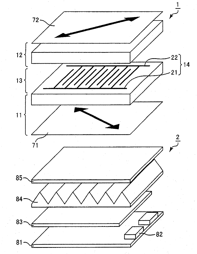
[0065] figure 1 It is a schematic perspective view of the liquid crystal display device of the first embodiment. The liquid crystal display device according to Embodiment 1 includes a liquid crystal display panel 1 including a liquid crystal layer 13 and a pair of substrates 11 and 12 sandwiching the liquid crystal layer 13 . More specifically, the liquid crystal display device of Embodiment 1 has these components in order from the back side toward the observation side, in the order of the TFT substrate 11 , the liquid crystal layer 13 , and the counter substrate 12 . The liquid crystal layer 13 contains a nematic liquid crystal having positive dielectric constant anisotropy (Δε>0). Furthermore, the liquid crystal display device according to Embodiment 1 includes a backlight unit 2 on the rear side of the liquid crystal display panel 1 .

[0066] Such as figure 1 As shown, the TFT substrate 11 in the above pair of substrates has a pair of comb-shaped electrodes 14 whose com...

Embodiment 1

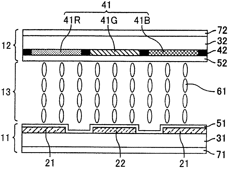
[0092] Figure 7 It is a schematic plan view of the sub-pixel unit in the display area of ​​the liquid crystal display device of the first embodiment. First, a pair of glass substrates is prepared, and an ITO film is formed on the entire surface of one of the glass substrates by sputtering. Next, a pair of ITO products with a width (electrode width) L of the lines 91 of the comb teeth of 2.5 μm and a width (electrode spacing) S of the intervals 92 between the comb teeth of 8 μm (that is, a pitch width P of 10.5 μm) were produced by photolithography. Comb electrodes.

[0093] Next, alignment film JALS-204 (5 wt %, γ-butyrolactone solution) manufactured by JSR Co., Ltd. was applied by spin coating on the comb-shaped electrodes and the glass substrate, followed by firing at 200° C. for 2 hours.

[0094] Next, on another glass substrate, a BM having a width of 10 μm, a length of 100 μm in the lateral direction, and a length of 300 μm in the vertical direction was formed, and an ...

Embodiment 2

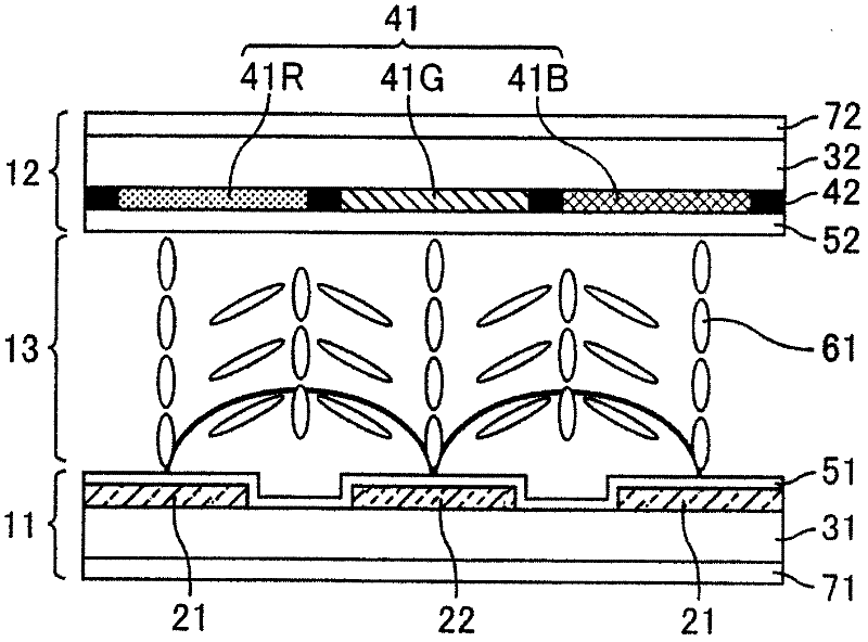
[0100] Figure 8 It is a schematic plan view of the sub-pixel unit in the display area of ​​the liquid crystal display device of the second embodiment. The liquid crystal display device of Example 2 was fabricated as follows: the width (electrode width) L of the lines 91 of the comb teeth was 2.5 μm, and the width (electrode spacing) S of the interval 92 between the comb teeth was 5 μm. It has the same structure as Example 1 except that the pitch width P is 7.5 micrometers.


PUM

PropertyMeasurementUnit
heightaaaaaaaaaa
heightaaaaaaaaaa
widthaaaaaaaaaa

Abstract

The present invention provides a liquid crystal display device in which the generation of moiré, which occurs when a voltage is applied, is suppressed in a liquid crystal mode in which a vertical alignment type liquid crystal is driven using at least one pair of comb-shaped electrodes. The liquid crystal display device of the present invention includes: a liquid crystal display panel having a liquid crystal layer and a pair of substrates sandwiching the liquid crystal layer; and a backlight unit disposed on the back side of the liquid crystal display panel, wherein one of the pair of substrates is The substrate has a pair of comb-shaped electrodes whose comb teeth are alternately meshed with each other. The above-mentioned liquid crystal layer contains liquid crystal molecules with positive dielectric constant anisotropy. Orientate in a direction perpendicular to the surface of one of the substrates, the above-mentioned backlight unit has an optical sheet with a plurality of fold lines parallel to each other on the surface, and the pitch width of the pair of comb-shaped electrodes is the same as the pitch width of the fold lines of the above-mentioned optical sheet is a non-integer multiple relationship.

Description

technical field [0001] The present invention relates to a liquid crystal display device. More specifically, it relates to a liquid crystal display device of a mode in which liquid crystal molecules are initially aligned vertically and an electric field (for example, a lateral electric field) is generated to control the liquid crystal molecules. Background technique [0002] Liquid crystal display devices are characterized by thinness, light weight, and low power consumption, and are widely used in various fields. In general, a backlight unit is mounted in a liquid crystal display device for display. Although it can be used as a light source to reflect sunlight for display, it is a liquid crystal display device mainly used indoors or a liquid crystal display device used outdoors that often requires a certain amount of brightness in word processors, notebook personal computers, and vehicle displays. , it is necessary to include a backlight unit with a light source in the str...

Claims


Application Information

Patent Timeline
Patent Type & Authority Applications(China)
IPC IPC(8): G02F1/13357G02F1/1337G02F1/1343
CPCG02F2001/133607G02F1/134363G02F1/133607
Inventor 村田充弘石原将市神崎修一樱井猛久中村正子大竹忠
Owner SHARP KK
Why Eureka
Try Eureka