Pixel structure and forming method of in-cell touch display panel

A touch display panel and pixel structure technology, applied in static indicators, data processing input/output process, optics, etc., can solve problems such as brightness drop and affect display quality, and achieve the effect of slight brightness reduction

Active Publication Date: 2011-12-28
HANNSTAR DISPLAY CORPORATION
View PDF4 Cites 17 Cited by
  • Summary
  • Abstract
  • Description
  • Claims
  • Application Information

AI Technical Summary

Problems solved by technology

However, this method will cause a decrease

Method used


Image

  • Pixel structure and forming method of in-cell touch display panel
  • Pixel structure and forming method of in-cell touch display panel
  • Pixel structure and forming method of in-cell touch display panel

Examples


Embodiment Construction

[0014] Certain terms are used in the specification and following claims to refer to particular elements. Those skilled in the art should understand that manufacturers may use different terms to refer to the same component. This description and the following claims do not use the difference in name as the way to distinguish components, but the difference in function of the components as the basis for the difference. The "comprising" mentioned throughout the specification and the following claims is an open-ended term, so it should be interpreted as "including but not limited to".

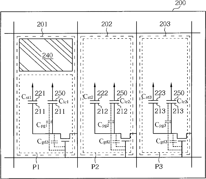
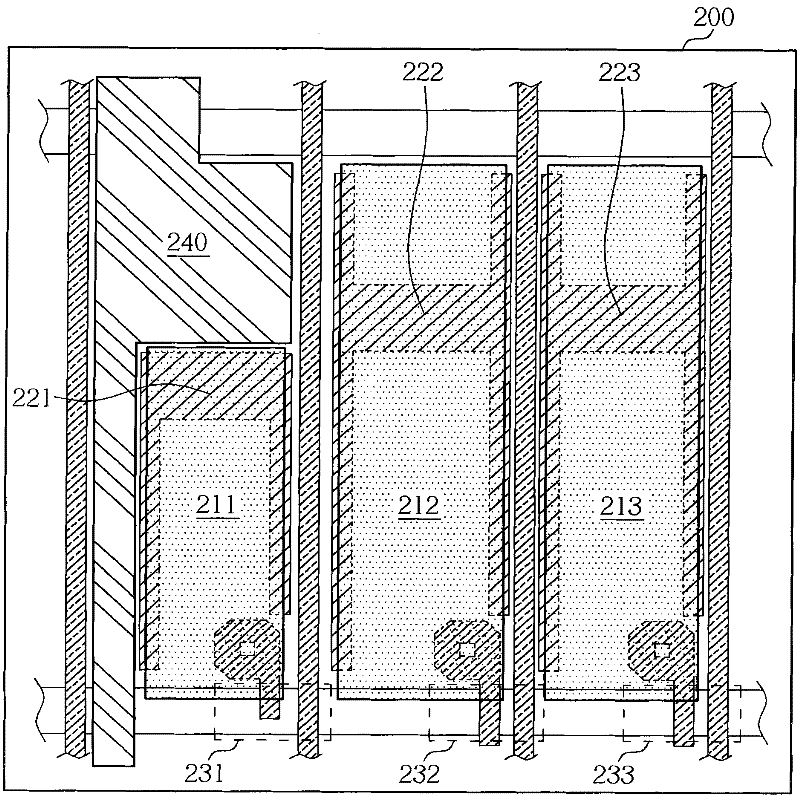
[0015] Please refer to figure 2 . figure 2 A partial equivalent circuit diagram of the pixel structure of the in-cell touch display panel according to the first preferred embodiment of the present invention is shown. Such as figure 2 As shown, the pixel structure of the in-cell touch display panel of this embodiment includes a substrate 200 and a plurality of sub-pixels, such as a first-time p...


PUM


Abstract

The invention provides a pixel structure of an embedded touch display panel. The pixel structure comprises a substrate on which a plurality of subpixel regions are defined and a plurality of subpixels, wherein the subpixels are respectively arranged in the subpixel regions; the transmitting area of at least one subpixel is different from the transmitting areas of the other subpixels in size; each subpixel comprises a liquid crystal capacitor with liquid crystal capacitance Clc, a storage capacitor with storage capacitance Cst and a thin film transistor with capacitance Cgd between a grid electrode and a drain electrode and capacitance Cpg between a grid electrode and a pixel electrode; each subpixel has capacitance ratio which is defined as (Cpg+Cgd)/(Cst+Clc+Cgd+Cpg) respectively; and the capacitance ratios of all the subpixels are the same in general.

Description

technical field [0001] The present invention relates to a pixel structure of an in-cell touch display panel and a method for forming the same, in particular to the use of adjusting the capacitance ratio (C pg +C gd ) / (C st +C lc +C gd +C pg ), a pixel structure of an in-cell touch display panel and a forming method thereof to solve electrical problems derived from pixels with different light-transmitting areas. Background technique [0002] Recently, since the touch display panel (touch display panel) is more and more widely used, the technology of the embedded touch sensor (touch sensor) is also paid more and more attention. The in-cell touch sensing element is directly manufactured in each pixel, and it is unavoidable to sacrifice part of the aperture ratio. In the known technology, a common practice is to reduce the area of ​​the red sub-pixel, the green sub-pixel, and the blue sub-pixel in equal proportions, and the extra area is used to place the touch sensing ele...

Claims


Application Information

Patent Timeline
IPC IPC(8): G02F1/133G02F1/1362G06F3/041
Inventor 任珂锐张弘昌吴昭慧
Owner HANNSTAR DISPLAY CORPORATION
Why Eureka
Try Eureka