Package for semiconductor device, and method for manufacturing the same and semiconductor device
一种光半导体装置、制造方法的技术,应用在半导体器件、半导体/固态器件零部件、电固体器件等方向,能够解决密封树脂27不足、外观缺陷、连接不良等问题
- Summary
- Abstract
- Description
- Claims
- Application Information
AI Technical Summary
Problems solved by technology
Method used
Image

Examples
Embodiment 1
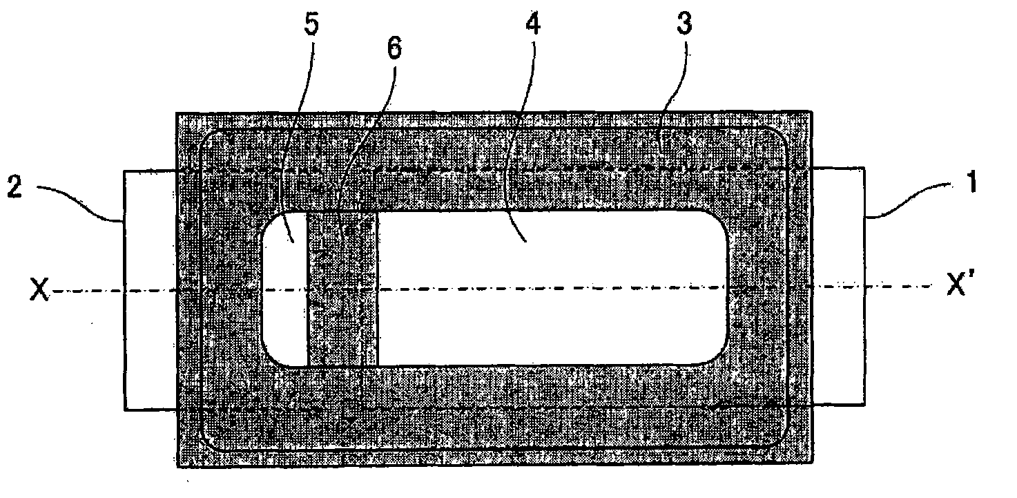
[0044] First, use Figure 1A ~ Figure 1C , Figure 2A ~ Figure 2D , the structure and manufacturing method of the semiconductor device package in Embodiment 1 will be described.
[0045] Figure 1A ~ Figure 1C It is a figure which shows the structure of the package for semiconductor devices in Example 1, Figure 1A is a top view, Figure 1B yes Figure 1A X-X' section view in Figure 1C It is a bottom view. Figure 2A ~ Figure 2D It is a process sectional view showing the manufacturing process of the package for semiconductor devices of this invention.
[0046] exist Figure 1A ~ Figure 1C Among them, reference numeral 1 is a lead frame having a mounting region 4 for a semiconductor element for the internal lead, reference numeral 2 is a lead frame having a connection region 5 connected to a semiconductor device for the internal lead, and reference numeral 3 is a lead frame formed between the lead frame 1 and the lead frame. 2 to hold them and surround the loading area 4...
Embodiment 2
[0056] Next, use Figure 3A ~ Figure 3D , the structure of the semiconductor device package in Example 2 will be described.
[0057] Figure 3A ~ Figure 3D It is a figure which shows the structure of the package for semiconductor devices in Example 2, and is a figure which shows the structural example of a step.
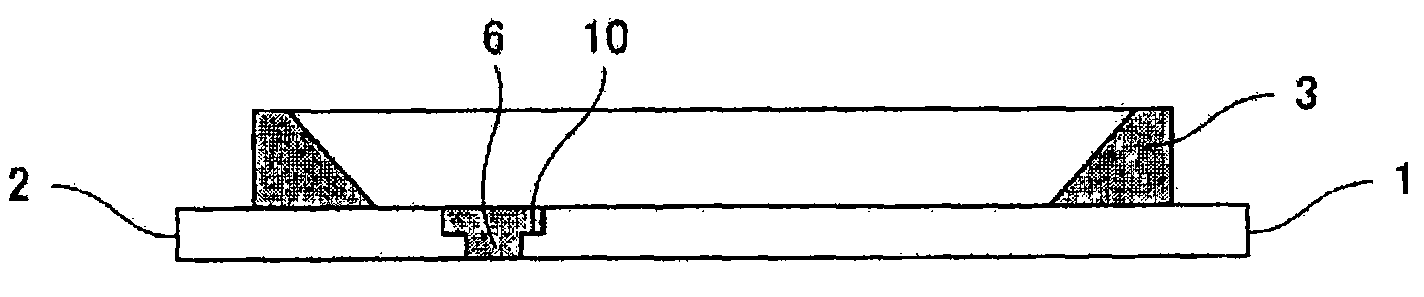
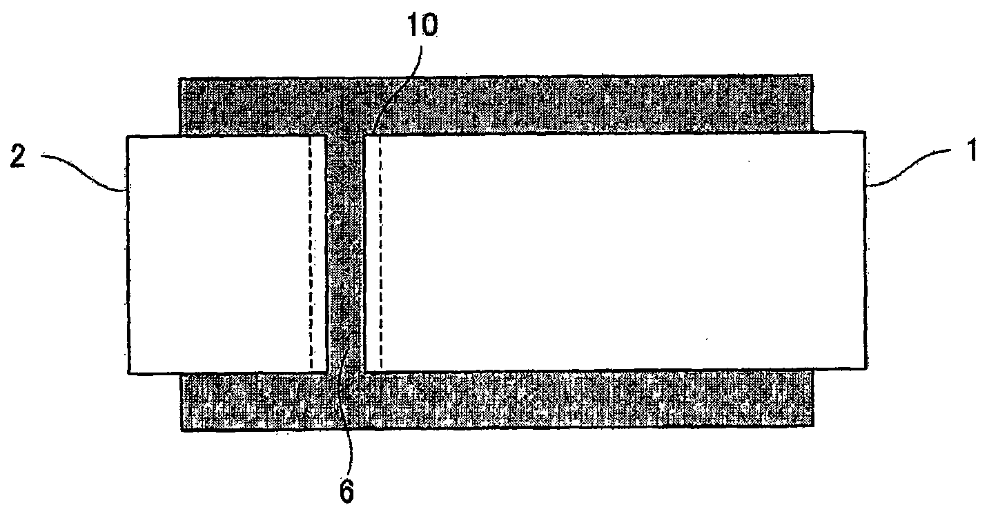
[0058] In Example 1, a structure is adopted in which a step 10 is provided on the upper surface side of the semiconductor element mounting surface of the lead frames 1 and 2, and a thinner part of the lead frame is left on the back surface opposite to the upper surface. , but if Figure 3A As shown, it is also possible to adopt the following structure: that is, between the opposite side surfaces of the lead frames 1, 2, at least the part exposed from the resin part 3 to the inside of the opening, on the back surface of the lead frames 1, 2 opposite to the upper surface Step 11 is set. Even in the case where the step 11 is provided on the back side, the gap betwee...
Embodiment 3
[0066] Next, use Figure 4A ~ Figure 4C , the structure of the semiconductor device package in Example 3 will be described.
[0067] Figure 4A ~ Figure 4C It is a figure which shows the structure of the resin between the lead frames in the package for semiconductor devices of Example 3, Figure 4A is a perspective view of main parts illustrating a case where protrusions are provided as an example of unevenness, Figure 4B It is a perspective view of main parts illustrating a case where a depression is provided as an example of unevenness, Figure 4C It is a perspective view of main parts showing an example of a case where grooves are provided as unevenness.
[0068] The semiconductor device package in Example 3 is characterized in that unevenness is formed on the surface of the holding resin 6 of the semiconductor device package in Example 1 or Example 2 exposed between the lead frames 1 and 2 .
[0069] Such as Figure 4A ~ Figure 4C As shown, the resin part 3 surrounds...
PUM
 Abstract
Description
Claims
Application Information
 - R&D
- Intellectual Property
- Life Sciences
- Materials
- Tech Scout
- Unparalleled Data Quality
- Higher Quality Content
- 60% Fewer Hallucinations
Browse by: Latest US Patents, China's latest patents, Technical Efficacy Thesaurus, Application Domain, Technology Topic, Popular Technical Reports.
© 2025 PatSnap. All rights reserved.Legal|Privacy policy|Modern Slavery Act Transparency Statement|Sitemap|About US| Contact US: help@patsnap.com