Chip-packaging structure, packaging method and electronic equipment

A chip packaging structure and chip packaging technology, applied in circuits, electrical components, electrical solid devices, etc., can solve the problem of easy falling off of the shielding film, and achieve the effect of not falling off easily and improving the anti-interference ability.

Inactive Publication Date: 2012-01-11
HUAWEI DEVICE CO LTD
View PDF4 Cites 12 Cited by
  • Summary
  • Abstract
  • Description
  • Claims
  • Application Information

AI Technical Summary

Problems solved by technology

[0004] Embodiments of the present invention provide a chip packaging structure, packaging method, and electronic equipment to solve the problem that the shielding film formed by conductive paint in the chip packaging structure is easy to fall off

Method used


Image

  • Chip-packaging structure, packaging method and electronic equipment
  • Chip-packaging structure, packaging method and electronic equipment
  • Chip-packaging structure, packaging method and electronic equipment

Examples


Embodiment Construction

[0024] The following will clearly and completely describe the technical solutions in the embodiments of the present invention with reference to the accompanying drawings in the embodiments of the present invention. Obviously, the described embodiments are only some, not all, embodiments of the present invention. Based on the embodiments of the present invention, all other embodiments obtained by persons of ordinary skill in the art without making creative efforts belong to the protection scope of the present invention.

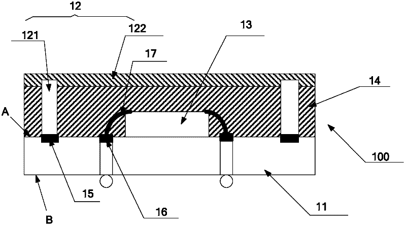
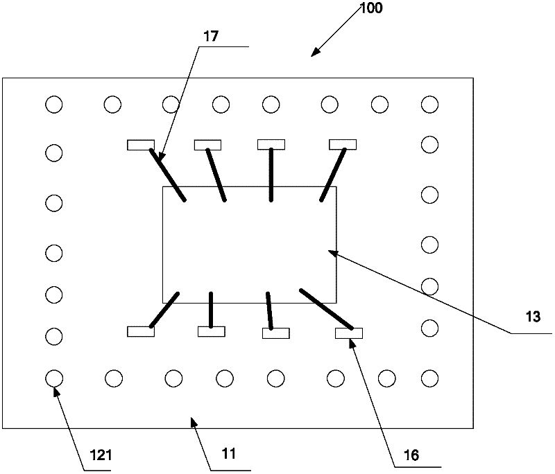
[0025] The chip packaging structure 100 provided by the embodiment of the present invention, such as figure 1 As shown, it includes a PCB (Printed Circuit Board, printed circuit board) 11 , a shielding case 12 , and a chip 13 to be shielded. Wherein, the shielding cover 12 is fixedly buckled on the part surface of the PCB board 11, that is, figure 1 On the middle A surface, the chip 13 to be shielded is arranged on the component surface of the PCB 11, located...


PUM


Abstract

The invention discloses a chip-packaging structure, a packaging method and electronic equipment, which relate to the field of chip packaging and are used for solving the problem that a shielding film formed from a conducting paint in the chip-packaging structure is easy to fall. The chip-packaging structure comprises a PCB (Printed Circuit Board), a shielding cover and a chip to be shielded, wherein the shielding cover is fixedly buckled on the part surface of the PCB; the chip to be shielded is arranged on the part surface of the PCB and positioned in the shielding cover, and the pipe feet of the chip to be shielded are connected with first welding disks on the PCB; and the chip to be shielded is not contacted with the shielding cover. The scheme provided by the invention can be applied to the packaging of the chip.

Description

technical field [0001] The invention relates to the field of chip packaging, in particular to a chip packaging structure, a packaging method and electronic equipment. Background technique [0002] In high-density packaging technology, the chip may be interfered by external electromagnetic signals, which may cause the performance of the chip to degrade or even be damaged, and cause the equipment where the chip is located to malfunction. [0003] At present, a chip packaging structure with a shielding function has appeared, and the chip packaging structure usually adopts the method of spraying conductive paint on the surface of the plastic packaged chip to shield the interference of external electromagnetic signals. However, the shielding film formed by the conductive paint in this chip packaging structure is easy to fall off, thereby reducing the anti-interference ability of this chip packaging structure, which also causes its unsatisfactory shielding function. Contents of ...

Claims


Application Information

Patent Timeline
Patent Type & Authority Applications(China)
IPC IPC(8): H01L23/552H01L21/50
CPCH01L2224/45144H01L2924/01013H01L25/00H01L2224/32225H01L21/56H01L2224/49171H01L2224/48227H01L24/48H01L2924/15311H01L2224/73265H01L24/49H01L2224/85H01L2924/15331H01L2924/3025H01L2224/45124H01L2924/19107H01L23/49838H01L2924/12041H01L23/552H01L24/45H01L24/73H01L2224/48091H01L2924/181H01L2224/48235H01L2924/00H01L2924/00012
Inventor 赵龙李春澍
Owner HUAWEI DEVICE CO LTD
Why Eureka
Try Eureka