Semiconductor light-emitting device provided with transparent organic supporting base plate and preparation method for semiconductor light-emitting device
A technology for supporting substrates and light-emitting devices, applied to semiconductor devices, electrical components, circuits, etc., to achieve the effects of reduced manufacturing costs, high light extraction efficiency, and low cost
- Summary
- Abstract
- Description
- Claims
- Application Information
AI Technical Summary
Problems solved by technology
Method used
Image
Examples
Embodiment 1
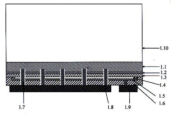
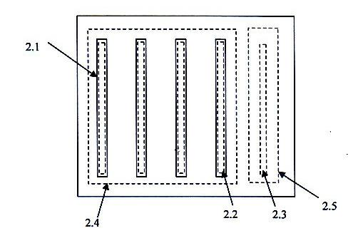
[0049] refer to figure 1 and figure 2 , to illustrate Embodiment 1 of the present invention.
[0050] First, a layer of semiconductor light-emitting layer: gallium nitride transition layer is grown on a sapphire growth substrate by metal organic chemical vapor deposition (MOCVD), and then N-type gallium nitride layer 1.1 (that is, N-type conductive layer) is grown sequentially. , an indium gallium nitrogen multiple quantum well layer 1.2 and a p-type gallium nitride layer 1.3 (that is, a p-type conductive layer), and the p-type gallium nitride layer 1.3 is activated by a thermal annealing process. Then on the surface of the P-type gallium nitride layer 1.3 (that is, the first surface of the semiconductor light-emitting stack) through a mask to form figure 2 The bar frame 2.1 shown by the solid line, and the P-type gallium nitride layer 1.3 and the indium gallium nitrogen multiple quantum well layer 1.2 in the bar frame 2.1 are removed by a reactive ion etching process unt...
Embodiment 2
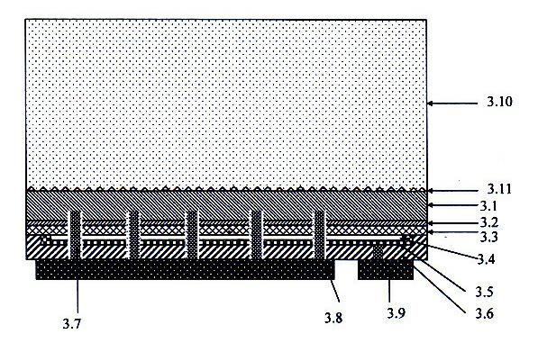
[0052] refer to image 3 and Figure 4 , to illustrate Embodiment 2 of the present invention.
[0053] First, a GaN transition layer is grown on a silicon growth substrate by metal-organic chemical vapor deposition (MOCVD), and then N-type GaN layer 3.1, InGaN multi-quantum well layer 3.2, P-type GaN layer 3.3, and activate the P-type GaN layer 3.3 through a thermal annealing process. Then on the surface of the P-type gallium nitride layer 3.3 through a mask to form Figure 4 The circular hole 4.1 shown by the solid line, and the P-type gallium nitride layer 3.3 and the multi-quantum well layer 3.2 in the circular hole 4.1 are removed by a reactive ion etching process until the N-type gallium nitride layer 3.1 is exposed. Then use the electron beam evaporation process to evaporate a layer of silver reflective ohmic electrode 3.4 on the surface of the sample, and use the photolithography process to make the reflective ohmic layer 3.4 only distributed on the surface of the P-...
PUM
 Abstract
Description
Claims
Application Information
 - R&D
- Intellectual Property
- Life Sciences
- Materials
- Tech Scout
- Unparalleled Data Quality
- Higher Quality Content
- 60% Fewer Hallucinations
Browse by: Latest US Patents, China's latest patents, Technical Efficacy Thesaurus, Application Domain, Technology Topic, Popular Technical Reports.
© 2025 PatSnap. All rights reserved.Legal|Privacy policy|Modern Slavery Act Transparency Statement|Sitemap|About US| Contact US: help@patsnap.com


