Megasonic cleaning head and megasonic cleaning system provided with same

A megasonic wave and cleaning head technology, which is applied in the field of semiconductor cleaning technology, can solve the problems of semiconductor damage, bending deformation roots, fractures, etc., and achieve the effect of small damage, elimination of inhomogeneity, and uniform distribution

Active Publication Date: 2013-12-18
BEIJING NAURA MICROELECTRONICS EQUIP CO LTD
View PDF11 Cites 0 Cited by
  • Summary
  • Abstract
  • Description
  • Claims
  • Application Information

AI Technical Summary

Problems solved by technology

However, there are still some defects in the control of the direction and uniformity of the megasonic energy. During the cleaning process, the energy generated perpendicular to the silicon grid makes it prone to bending deformation and even root fracture due to shear force, causing damage to the semiconductor.

Method used


Image

  • Megasonic cleaning head and megasonic cleaning system provided with same
  • Megasonic cleaning head and megasonic cleaning system provided with same
  • Megasonic cleaning head and megasonic cleaning system provided with same

Examples


Embodiment Construction

[0030] The specific implementation manners of the present invention will be further described in detail below in conjunction with the accompanying drawings and embodiments. The following examples serve to illustrate the present invention, but do not limit the scope of the present invention.

[0031] The megasonic cleaning head of the present invention includes: a transducer and a resonator, the resonator is used to propagate energy from the transducer; the resonator has an upper surface and a lower surface, the upper surface is coupled to the transducer, and the resonator The interior has an array of holes impermeable to the vacuum of the upper and lower surfaces.

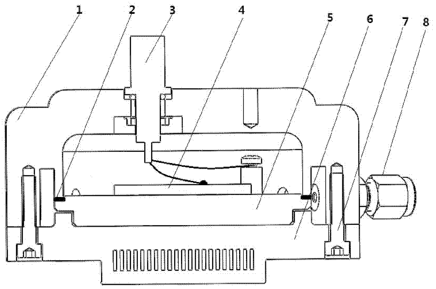
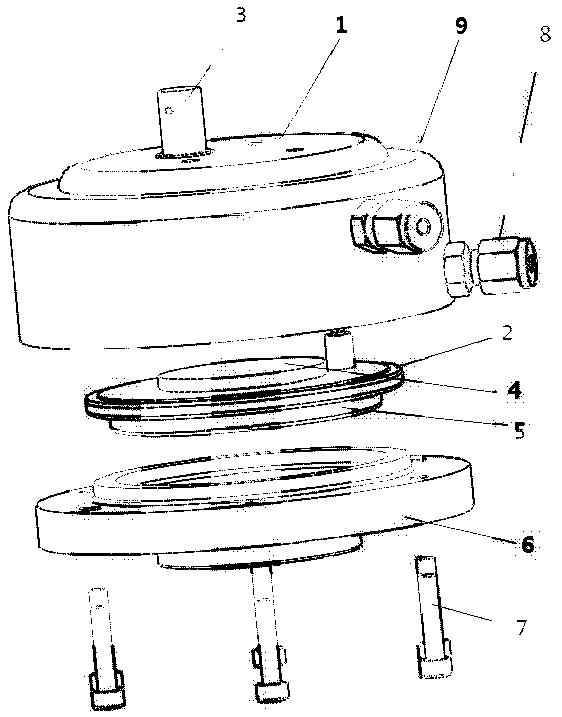
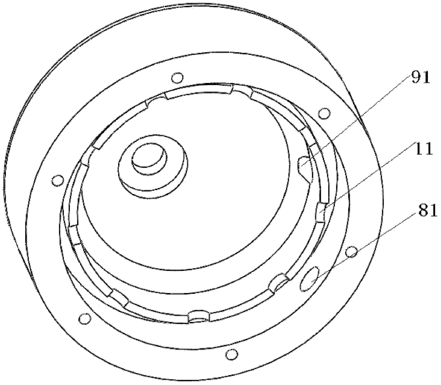
[0032] like Figure 1-2 As shown, an embodiment of the megasonic cleaning head of the present invention includes: an upper casing 1, a coupling layer and a lower casing 6; in this embodiment, the transducer includes an upper casing 1 and a coupling layer, and the resonator It is the lower shell 6; if Figure 1-3...


PUM


Abstract

The invention provides a megasonic cleaning head and a megasonic cleaning system provided with the same. The cleaning head comprises a transducer and a resonator which is used for transmitting energy from the transducer. The resonator comprises an upper surface and a lower surface and the upper surface is coupled to the transducer; and a vacuum hole array which not penetrates through the upper surface and the lower surface are arranged in the resonator. the megasonic cleaning head provided by the invention has the beneficial effect that, because of the adoption of the resonator internally provided with a non-through vacuum hole array in cylindrical shape or other geometrical shapes, the non-homogeneity of vibration waves is eliminated through compensating consumption effect achieved when megasonic waves are reflected many times in the resonator, so that the uniform distribution of megasonic energy is realized. When ultrapure water or chemical liquid is sprayed in a semiconductor, impurities on the semiconductor are washed off through uniform fluid waves which are generated by the megasonic wave and then the impurities are brought away by the flowing of the liquid, so that the semiconductor is cleaned and the damages to the semiconductor are smaller.

Description

technical field [0001] The invention relates to the field of semiconductor cleaning technology, in particular to a megasonic cleaning head and a megasonic cleaning system with the cleaning head. Background technique [0002] With the rapid development of submicron and deep submicron ultra-large-scale integrated circuits (ULSI) following "Moore's Law", the design line width has decreased sharply, and the volume of semiconductor chips has become smaller and smaller. How to control the mechanical damage of silicon wafer surface materials , and under the premise of protecting the flatness of the silicon wafer surface, minimizing the defect density of the silicon wafer and controlling its defect rate have become a major challenge in today's semiconductor cleaning technology. The structure of control electrodes and capacitors below the 65nm node becomes more and more fragile. As the line width of integrated circuits becomes smaller and smaller, the particles that can affect the d...

Claims


Application Information

Patent Timeline
Patent Type & Authority Patents(China)
IPC IPC(8): B08B3/12
Inventor 初国超吴仪
Owner BEIJING NAURA MICROELECTRONICS EQUIP CO LTD
Why Eureka
Try Eureka