Electrode structure of display panel and electrode forming method using dummy electrode

a technology of electrode forming and display panel, which is applied in the manufacture of electric discharge tubes/lamps, identification means, instruments, etc., to achieve the effect of removing the non-uniformity of electrical characteristics

Inactive Publication Date: 2004-01-20
FUJITSU HITACHI PLASMA DISPLAY LTD
View PDF5 Cites 23 Cited by
  • Summary
  • Abstract
  • Description
  • Claims
  • Application Information

AI Technical Summary

Benefits of technology

In consideration of such circumstances, it is an object of the present invention to provide an electrode structure of a display panel in which a dummy electrode for limiting the flow of etching solvent is provided in a block boundary portion at a substrate end to prevent excessive etching of an electrode material layer positioned in the block boundary portion and after manufacture, the dummy electrode is utilized also for correction of nonuniform coupling capacity, thereby eliminating the nonuniformity of electrical characteristics which would otherwise be involved with the discontinuity in the intervals between terminals, and an electrode forming method.
According to the present invention, a fine electrode pattern can be fabricated more uniformly with high precision. Consequently, it is possible to prevent display unevenness in the block boundary portion. Moreover, in the case in which a coupling portion for coupling the dummy electrode and the lead electrode portion is provided, the coupling capacity of the electrodes is almost equal in all the electrodes. Therefore, it is possible to obtain a display panel having uniform electrical characteristics.

Problems solved by technology

However, when the electrode material layer is etched by the spray etching method while delivering the substrate by means of the inline manufacturing system, the etching solvent is excessively supplied to a block boundary portion B of the resist pattern formed on the electrode material layer and the electrode material layer is over-etched in this portion.
This difference in the electrode distances (i.e., in the density of the electrodes) at the end of the substrate causes a problem during etching.

Method used


Image

  • Electrode structure of display panel and electrode forming method using dummy electrode
  • Electrode structure of display panel and electrode forming method using dummy electrode
  • Electrode structure of display panel and electrode forming method using dummy electrode

Examples


Embodiment Construction

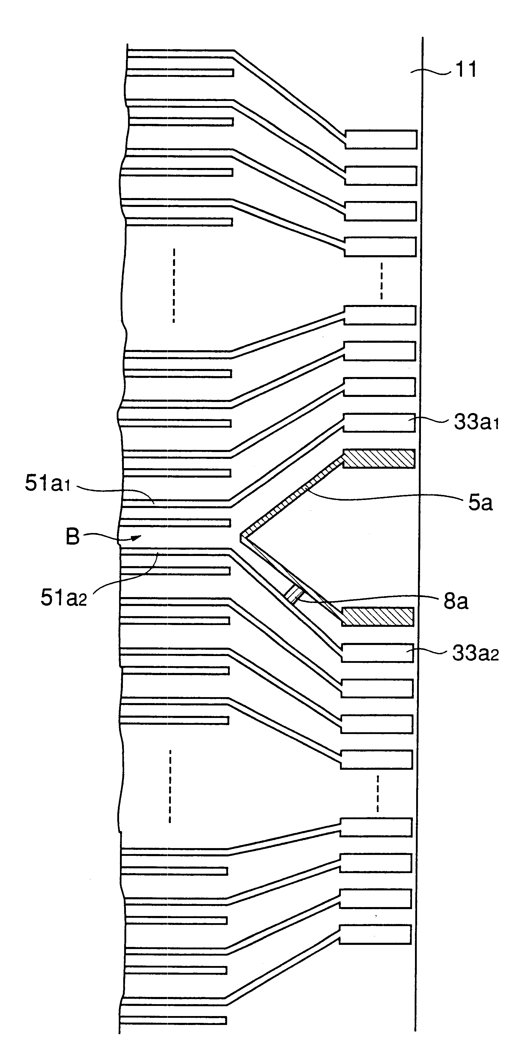
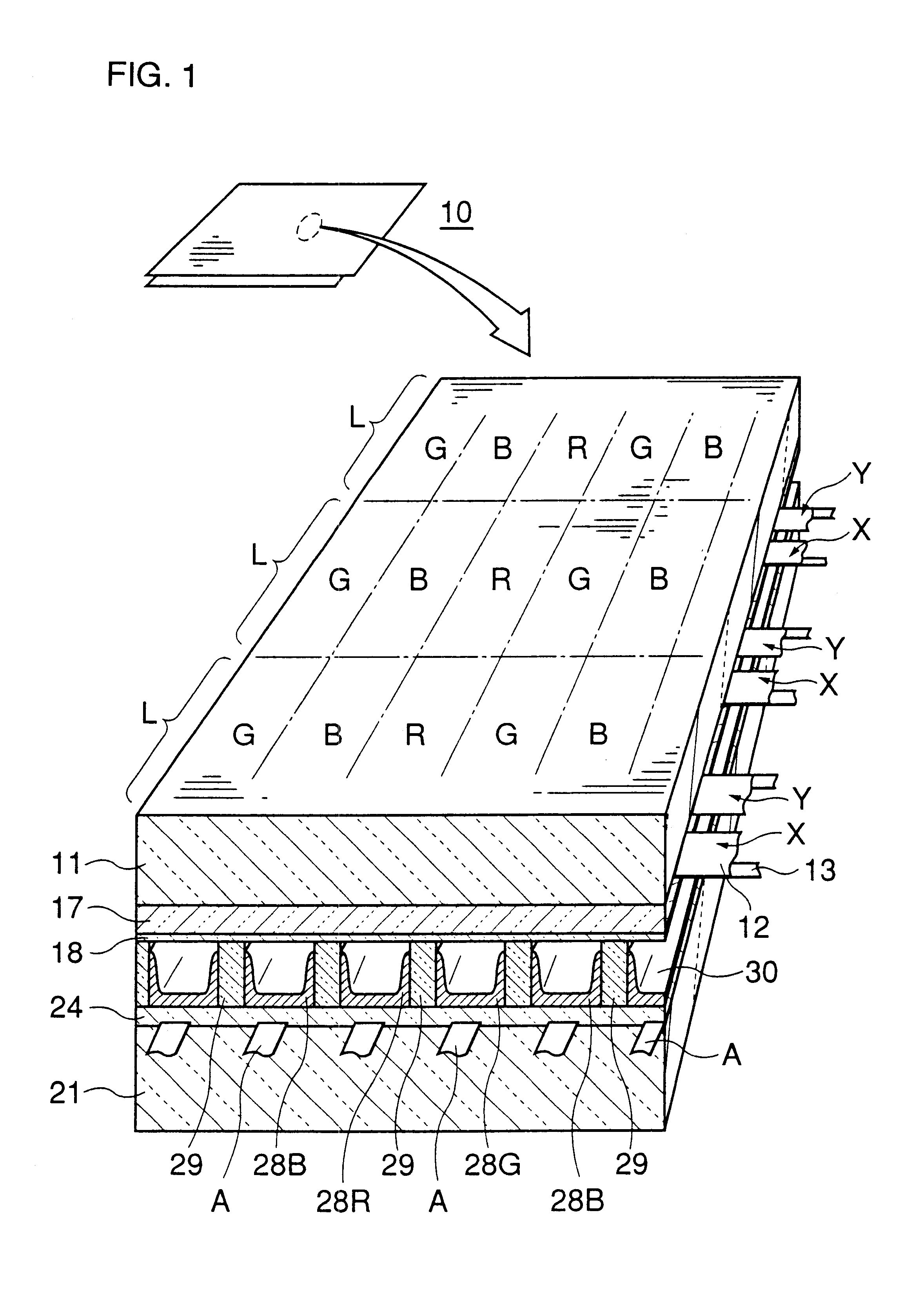
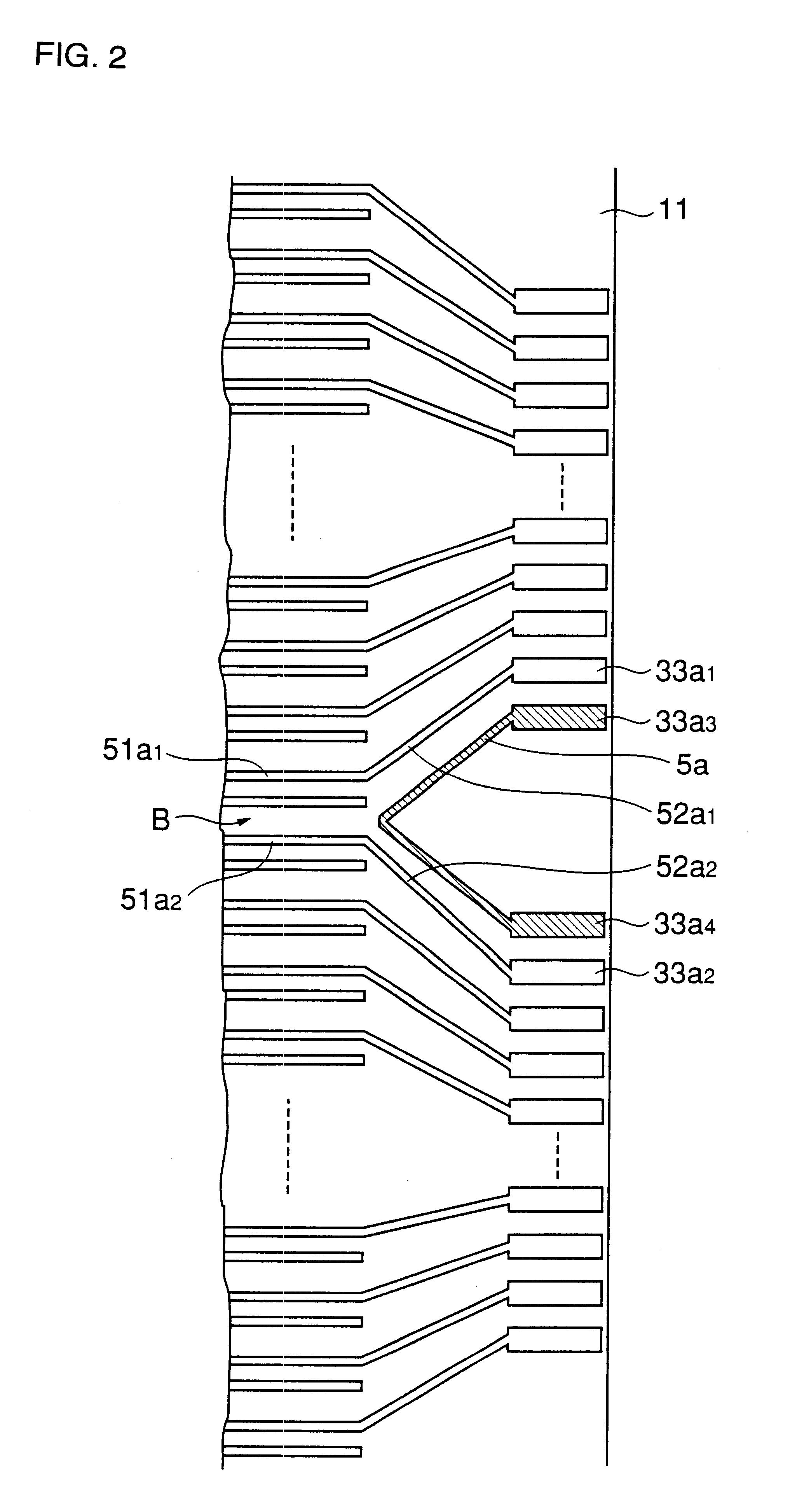
In the present invention, the substrate constituting the display panel may be a substrate of glass, quartz, ceramic or the like, on which a desired structure such as electrodes, an insulating film, a dielectric layer or a protective film may or may not be formed.

It is sufficient that the electrode is constituted by the display electrode portion and the lead electrode portion. The electrode may be formed of any known electrode material by any known process in the field without particular limitation. Examples of electrode materials include ITO, SnO.sub.2, Ag, Au, Al, Cu, Cr, and their alloys and multilayered structures (for example, a Cr / Cu / Cr multilayered structure) and the like. As an electrode forming method, for example, an electrode material layer is uniformly formed on the substrate by a film formation technique such as evaporation or sputtering, a resist pattern having the geometry of the electrodes is formed on the electrode material layer by photolithography or the like, and ...


PUM

PropertyMeasurementUnit
widthaaaaaaaaaa
timeaaaaaaaaaa
sizeaaaaaaaaaa

Abstract

An electrode structure of a display panel includes a plurality of electrodes formed on a substrate constituting the display panel, the electrodes including display electrode portions provided in almost parallel in a central part of the substrate and oblique lead electrode portions converged in a predetermined number for each block from the display electrode portions to reach terminal portions at an end of the substrate, and a dummy electrode provided between two oblique lead electrode portions extending in different directions in a block boundary portion for limiting a flow of an etching solvent into the block boundary portion during etching when the electrodes are formed.

Description

BACKGROUND OF THE INVENTION1. Field of the InventionThe present invention relates to an electrode structure of a display panel and an electrode forming method, and more particularly, to an electrode structure of a display panel, for example, a plasma display panel (PDP), a liquid crystal display panel (LCD), an electro luminescence display (EL) or the like, in which electrodes are formed on a substrate through etching, and an electrode forming method.2. Description of the Related ArtIn a display panel of this kind, generally, electrodes are often formed through etching. In the case where the electrodes are to be formed on the substrate through etching, first, a layer of an electrode material such as ITO, SnO.sub.2, Cr, Cu or Ag is uniformly formed over the whole surface of the substrate by evaporation, sputtering or printing such as slot coating, then a resist pattern having a geometry of the electrodes is formed on the electrode material layer by photolithography or the like, and t...

Claims


Application Information

Patent Timeline
Patent Type & Authority Patents(United States)
IPC IPC(8): G02F1/13G02F1/1345H01J9/24H01J17/02H01J17/18H05K3/06H05K1/11H01J11/46G02F1/1333G09F9/00G09F9/30H01J9/02H01J11/12H01J11/22H01J11/24H01J11/26H01J11/34H01J11/48
CPCG02F1/1345H01J9/241H01J17/18H01J2217/49H05K1/117H05K3/06
Inventor OGAWA, TETSUYA
Owner FUJITSU HITACHI PLASMA DISPLAY LTD
Why Eureka
Try Eureka